参数资料
| 型号: | LTC2205IUK-14#PBF |
| 厂商: | Linear Technology |
| 文件页数: | 13/28页 |
| 文件大小: | 0K |
| 描述: | IC ADC 14BIT 65MSPS 48-QFN |
| 标准包装: | 52 |
| 位数: | 14 |
| 采样率(每秒): | 65M |
| 数据接口: | 并联 |
| 转换器数目: | 1 |
| 功率耗散(最大): | 776mW |
| 电压电源: | 单电源 |
| 工作温度: | -40°C ~ 85°C |
| 安装类型: | 表面贴装 |
| 封装/外壳: | 48-WFQFN 裸露焊盘 |
| 供应商设备封装: | 48-QFN-EP(7x7) |
| 包装: | 管件 |
| 输入数目和类型: | 1 个差分 |
| 配用: | DC890B-ND - BOARD USB DATA COLLECTION |
第1页第2页第3页第4页第5页第6页第7页第8页第9页第10页第11页第12页当前第13页第14页第15页第16页第17页第18页第19页第20页第21页第22页第23页第24页第25页第26页第27页第28页
LTC2205-14
20
220514fb
The lower limit of the LTC2205-14 sample rate is determined
by droop of the sample and hold circuits. The pipelined
architecture of this ADC relies on storing analog signals on
small valued capacitors. Junction leakage will discharge
the capacitors. The specied minimum operating frequency
for the LTC2205-14 is 1Msps.
DIGITAL OUTPUTS
Digital Output Buffers
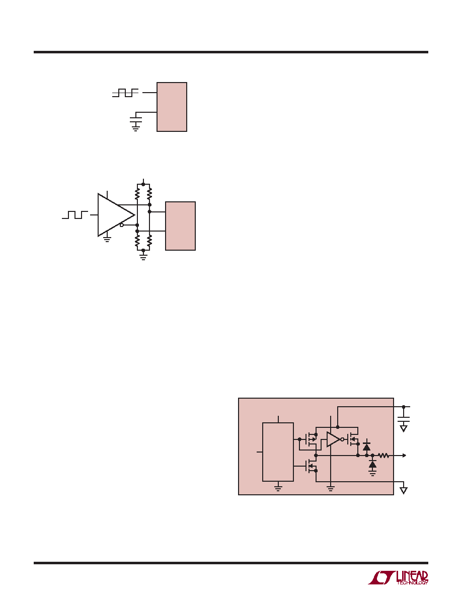
Figure 11 shows an equivalent circuit for a single output
buffer. Each buffer is powered by OVDD and OGND, isolated
from the ADC power and ground. The additional N-channel
transistor in the output driver allows operation down to
low voltages. The internal resistor in series with the output
eliminates the need for external damping resistors.
As with all high speed/high resolution converters, the
digital output loading can affect the performance. The
digital outputs of the LTC2205-14 should drive a minimum
capacitive load to avoid possible interaction between the
digital outputs and sensitive input circuitry. The output
should be buffered with a device such as a ALVCH16373
CMOS latch. For full speed operation the capacitive load
should be kept under 10pF. A resistor in series with the
output may be used but is not required since the ADC has
a series resistor of 33Ω on chip.
Lower OVDD voltages will also help reduce interference
from the digital outputs.
Maximum and Minimum Encode Rates
The maximum encode rate for the LTC2205-14 is 65Msps.
For the ADC to operate properly the encode signal should
have a 50% (±2.5%) duty cycle. Achieving a precise 50%
duty cycle is easy with differential sinusoidal drive using
a transformer or using symmetric differential logic such
as PECL or LVDS. When using a single-ended ENCODE
signal asymmetric rise and fall times can result in duty
cycles that are far from 50%.
An optional clock duty cycle stabilizer can be used if the
input clock does not have a 50% duty cycle. This circuit
uses the rising edge of ENC pin to sample the analog input.
The falling edge of ENC is ignored and an internal falling
edge is generated by a phase-locked loop. The input clock
duty cycle can vary from 30% to 70% and the clock duty
cycle stabilizer will maintain a constant 50% internal duty
cycle. If the clock is turned off for a long period of time,
the duty cycle stabilizer circuit will require one hundred
clock cycles for the PLL to lock onto the input clock. To
use the clock duty cycle stabilizer, the MODE pin must be
connected to 1/3VDD or 2/3VDD using external resistors.
APPLICATIONS INFORMATION
LTC2205-14
220514 F11
OVDD
VDD
0.1μF
TYPICAL
DATA
OUTPUT
OGND
OVDD
0.5V
TO 3.6V
PREDRIVER
LOGIC
DATA
FROM
LATCH
33Ω
Figure 11. Equivalent Circuit for a Digital Output Buffer
Figure 10. ENC Drive Using a CMOS to PECL Translator
Figure 9. Single-Ended ENC Drive,
Not Recommended for Low Jitter
220514 F09
ENC–
1.6V
VTHRESHOLD = 1.6V
ENC+
0.1μF
LTC2205-14
220514 F10
ENC–
ENC+
3.3V
D0
Q0
130Ω
83Ω
MC100LVELT22
LTC2205-14
相关PDF资料 |
PDF描述 |
|---|---|
| LTC2207IUK-14#PBF | IC ADC 14BIT 105MSPS 48-QFN |
| LTC2220IUP-1#TRPBF | IC ADC 12BIT 185MSPS 64-QFN |
| LTC2221IUP#TRPBF | IC ADC 12-BIT 135MSPS 64-QFN |
| LTC2222IUK-11#TRPBF | IC ADC 11BIT 105MSPS SAMPL 48QFN |
| LTC2223IUK#TRPBF | IC ADC 12BIT 80MSPS SAMPLE 48QFN |
相关代理商/技术参数 |
参数描述 |
|---|---|
| LTC2205IUK-PBF | 制造商:LINER 制造商全称:Linear Technology 功能描述:16-Bit, 65Msps/40Msps |
| LTC2205IUK-TR | 制造商:LINER 制造商全称:Linear Technology 功能描述:16-Bit, 65Msps/40Msps |
| LTC2205IUK-TRPBF | 制造商:LINER 制造商全称:Linear Technology 功能描述:16-Bit, 65Msps/40Msps |
| LTC2205UK | 制造商:LINER 制造商全称:Linear Technology 功能描述:16-Bit, 65Msps/40Msps |
| LTC2205UK-14 | 制造商:LINER 制造商全称:Linear Technology 功能描述:14-Bit, 65Msps ADC |
发布紧急采购,3分钟左右您将得到回复。