- 您现在的位置:买卖IC网 > PDF目录296330 > LTC2207CUK-14#PBF (LINEAR TECHNOLOGY CORP) 16-Bit, 105Msps ADC; Package: QFN; No of Pins: 48; Temperature Range: 0°C to +70°C PDF资料下载
参数资料
| 型号: | LTC2207CUK-14#PBF |
| 厂商: | LINEAR TECHNOLOGY CORP |
| 元件分类: | ADC |
| 英文描述: | 16-Bit, 105Msps ADC; Package: QFN; No of Pins: 48; Temperature Range: 0°C to +70°C |
| 中文描述: | 1-CH 14-BIT PROPRIETARY METHOD ADC, PARALLEL ACCESS, PQCC48 |
| 封装: | 7 X 7 MM, LEAD FREE, PLASTIC, MO-220WKKD-2, QFN-48 |
| 文件页数: | 10/32页 |
| 文件大小: | 1237K |
| 代理商: | LTC2207CUK-14#PBF |
第1页第2页第3页第4页第5页第6页第7页第8页第9页当前第10页第11页第12页第13页第14页第15页第16页第17页第18页第19页第20页第21页第22页第23页第24页第25页第26页第27页第28页第29页第30页第31页第32页
LTC2207-14/LTC2206-14
18
220714614fc
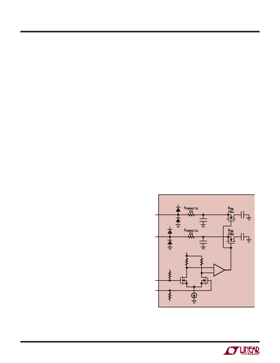
Figure 2. Equivalent Input Circuit
CSAMPLE
4.9pF
VDD
LTC2207-14/LTC2206-14
AIN+
2207614 F02
CSAMPLE
4.9pF
VDD
AIN–
ENC–
ENC+
1.6V
6k
1.6V
6k
CPARASITIC
1.8pF
CPARASITIC
1.8pF
SAMPLE/HOLD OPERATION AND INPUT DRIVE
Sample/Hold Operation
Figure 2 shows an equivalent circuit for the LTC2207-14/
LTC2206-14 CMOS differential sample and hold. The dif-
ferential analog inputs are sampled directly onto sampling
capacitors (CSAMPLE) through NMOS transistors. The
capacitors shown attached to each input (CPARASITIC) are
the summation of all other capacitance associated with
each input.
During the sample phase when ENC is low, the NMOS
transistors connect the analog inputs to the sampling
capacitors and they charge to, and track the differential
input voltage. When ENC transitions from low to high, the
sampled input voltage is held on the sampling capacitors.
During the hold phase when ENC is high, the sampling
capacitors are disconnected from the input and the held
voltage is passed to the ADC core for processing. As ENC
transitions from high to low, the inputs are reconnected to
the sampling capacitors to acquire a new sample. Since
the sampling capacitors still hold the previous sample,
a charging glitch proportional to the change in voltage
between samples will be seen at this time. If the change
between the last sample and the new sample is small,
the charging glitch seen at the input will be small. If the
input change is large, such as the change seen with input
frequencies near Nyquist, then a larger charging glitch
will be seen.
Common Mode Bias
The ADC sample-and-hold circuit requires differential
drive to achieve specied performance. Each input should
swing ±0.5625V for the 2.25V range (PGA = 0) or ±0.375V
for the 1.5V range (PGA = 1), around a common mode
voltage of 1.25V. The VCM output pin (Pin 2) is designed
to provide the common mode bias level. VCM can be tied
directly to the center tap of a transformer to set the DC
input level or as a reference level to an op amp differential
driver circuit. The VCM pin must be bypassed to ground
close to the ADC with a 2.2μF capacitor or greater.
Input Drive Impedance
As with all high performance, high speed ADCs the dy-
namic performance of the LTC2207-14/LTC2206-14 can
be inuenced by the input drive circuitry, particularly
the second and third harmonics. Source impedance and
input reactance can inuence SFDR. At the falling edge
of ENC the sample-and-hold circuit will connect the 4.9pF
sampling capacitor to the input pin and start the sampling
period. The sampling period ends when ENC rises, hold-
ing the sampled input on the sampling capacitor. Ideally,
the input circuitry should be fast enough to fully charge
the sampling capacitor during the sampling period
1/(2FENCODE); however, this is not always possible and the
incomplete settling may degrade the SFDR. The sampling
glitch has been designed to be as linear as possible to
minimize the effects of incomplete settling.
For the best performance it is recommended to have a
source impedance of 100
Ω or less for each input. The
source impedance should be matched for the differential
inputs. Poor matching will result in higher even order
harmonics, especially the second.
APPLICATIONS INFORMATION
相关PDF资料 |
PDF描述 |
|---|---|
| LTC2207CUK-14#TRPBF | 16-Bit, 105Msps ADC; Package: QFN; No of Pins: 48; Temperature Range: 0°C to +70°C |
| LTC2207IUK-14#PBF | 16-Bit, 105Msps ADC; Package: QFN; No of Pins: 48; Temperature Range: -40°C to +85°C |
| LTC2207IUK-14#TRPBF | 16-Bit, 105Msps ADC; Package: QFN; No of Pins: 48; Temperature Range: -40°C to +85°C |
| LTC2206CUK#PBF | 16-Bit, 80Msps ADC; Package: QFN; No of Pins: 48; Temperature Range: 0°C to +70°C |
| LTC2206CUK#TRPBF | 16-Bit, 80Msps ADC; Package: QFN; No of Pins: 48; Temperature Range: 0°C to +70°C |
相关代理商/技术参数 |
参数描述 |
|---|---|
| LTC2207IUK | 制造商:Linear Technology 功能描述:ADC Single Pipelined 105Msps 16-bit Parallel 48-Pin QFN EP |
| LTC2207IUK#PBF | 制造商:Linear Technology 功能描述:ADC Single Pipelined 105Msps 16-bit Parallel 48-Pin QFN EP 制造商:Linear Technology 功能描述:IC ADC 16-BIT 105MSPS 48-QFN 制造商:Linear Technology 功能描述:ADC 16BIT 105MSPS 48QFN 制造商:Linear Technology 功能描述:IC, ADC, 16BIT, 105MSPS, QFN-48; Resolution (Bits):16bit; Sampling Rate:105MSPS; Supply Voltage Type:Single; Supply Voltage Min:3.135V; Supply Voltage Max:3.465V; Supply Current:273mA; Digital IC Case Style:QFN; No. of Pins:48 ;RoHS Compliant: Yes |
| LTC2207IUK#TRPBF | 制造商:Linear Technology 功能描述:ADC Single Pipelined 105Msps 16-bit Parallel 48-Pin QFN EP T/R 制造商:Linear Technology 功能描述:IC ADC 16BIT 105MSPS 48-QFN |
| LTC2207IUK-14 | 制造商:Linear Technology 功能描述:ADC Single Pipelined 105Msps 14-bit Parallel 48-Pin QFN EP |
| LTC2207IUK-14#PBF | 功能描述:IC ADC 14BIT 105MSPS 48-QFN RoHS:是 类别:集成电路 (IC) >> 数据采集 - 模数转换器 系列:- 产品培训模块:Lead (SnPb) Finish for COTS Obsolescence Mitigation Program 标准包装:250 系列:- 位数:12 采样率(每秒):1.8M 数据接口:并联 转换器数目:1 功率耗散(最大):1.82W 电压电源:模拟和数字 工作温度:-40°C ~ 85°C 安装类型:表面贴装 封装/外壳:48-LQFP 供应商设备封装:48-LQFP(7x7) 包装:管件 输入数目和类型:2 个单端,单极 |
发布紧急采购,3分钟左右您将得到回复。