参数资料
| 型号: | LTC2207IUK-14#PBF |
| 厂商: | Linear Technology |
| 文件页数: | 18/32页 |
| 文件大小: | 0K |
| 描述: | IC ADC 14BIT 105MSPS 48-QFN |
| 标准包装: | 52 |
| 位数: | 14 |
| 采样率(每秒): | 105M |
| 数据接口: | 并联 |
| 转换器数目: | 1 |
| 功率耗散(最大): | 1.07W |
| 电压电源: | 单电源 |
| 工作温度: | -40°C ~ 85°C |
| 安装类型: | 表面贴装 |
| 封装/外壳: | 48-WFQFN 裸露焊盘 |
| 供应商设备封装: | 48-QFN-EP(7x7) |
| 包装: | 管件 |
| 输入数目和类型: | 1 个差分 |
| 配用: | DC890B-ND - BOARD USB DATA COLLECTION |
第1页第2页第3页第4页第5页第6页第7页第8页第9页第10页第11页第12页第13页第14页第15页第16页第17页当前第18页第19页第20页第21页第22页第23页第24页第25页第26页第27页第28页第29页第30页第31页第32页
LTC2207-14/LTC2206-14
25
220714614fc
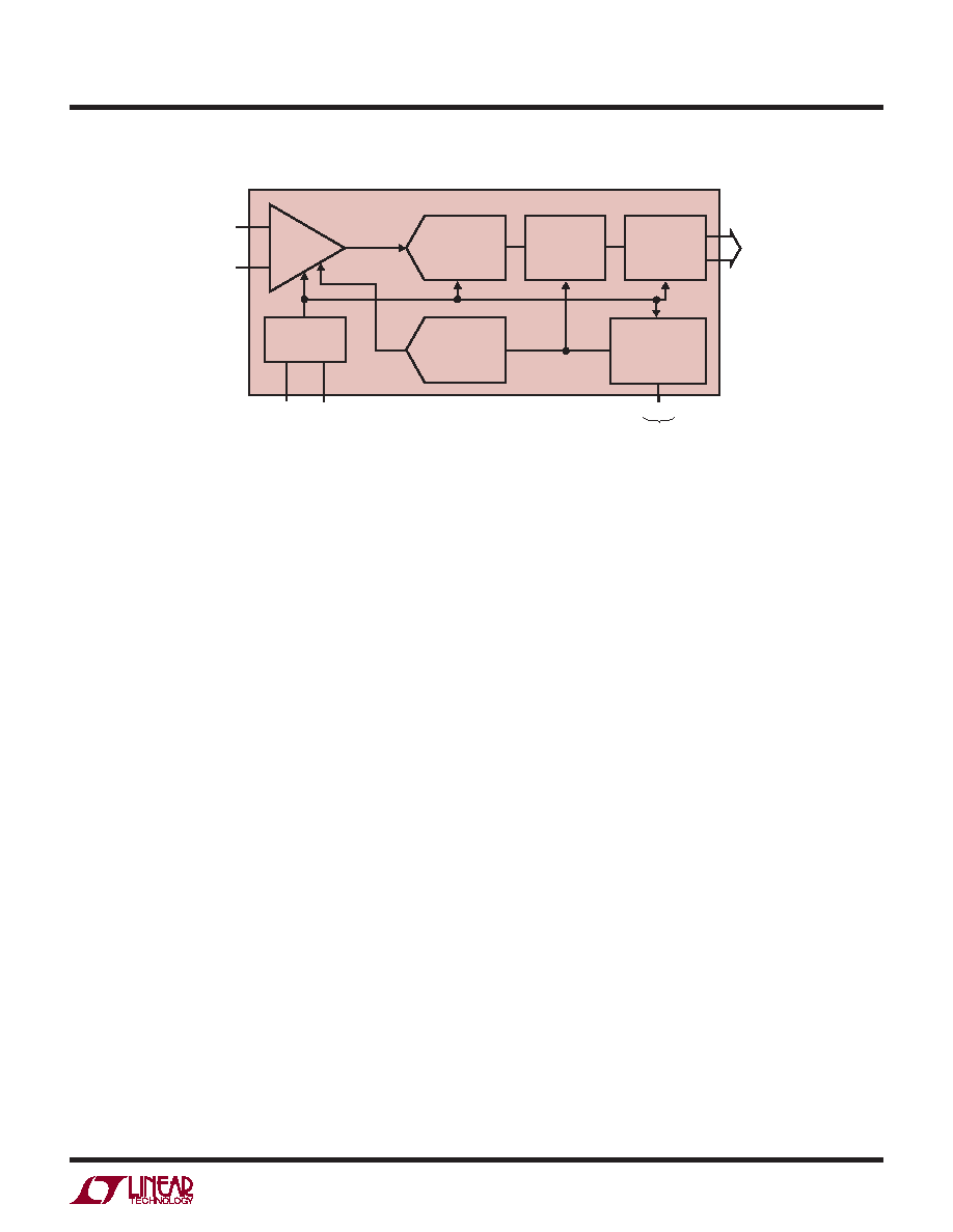
Figure 14. Functional Equivalent Block Diagram of Internal Dither Circuit
+–
AIN–
AIN+
S/H
AMP
DIGITAL
SUMMATION
OUTPUT
DRIVERS
MULTIBIT DEEP
PSEUDO-RANDOM
NUMBER
GENERATOR
14-BIT
PIPELINED
ADC CORE
PRECISION
DAC
CLOCK/DUTY
CYCLE
CONTROL
CLKOUT
OF
D13
D0
ENC
DITHER ENABLE
HIGH = DITHER ON, LOW = DITHER OFF
DITH
ENC
ANALOG
INPUT
2207614 F14
LTC2207-14/LTC2206-14
As shown in Figure 14, the output of the sample-and-hold
amplier is summed with the output of a dither DAC. The
dither DAC is driven by a long sequence pseudo-random
number generator; the random number fed to the dither
DAC is also subtracted from the ADC result. If the dither
DAC is precisely calibrated to the ADC, very little of the
dither signal will be seen at the output. The dither signal
that does leak through will appear as white noise. The dither
DAC is calibrated to result in less than 0.5dB elevation in
the noise oor of the ADC, as compared to the noise oor
with dither off.
Grounding and Bypassing
The LTC2207-14/LTC2206-14 require a printed circuit board
with a clean unbroken ground plane; a multilayer board
with an internal ground plane is recommended. The pinout
of the LTC2207-14/LTC2206-14 has been optimized for a
owthrough layout so that the interaction between inputs
and digital outputs is minimized. Layout for the printed
circuit board should ensure that digital and analog signal
lines are separated as much as possible. In particular, care
should be taken not to run any digital track alongside an
analog signal track or underneath the ADC.
High quality ceramic bypass capacitors should be used
at the VDD, VCM, and OVDD pins. Bypass capacitors must
be located as close to the pins as possible. The traces
connecting the pins and bypass capacitors must be kept
short and should be made as wide as possible.
The LTC2207-14/LTC2206-14 differential inputs should run
parallel and close to each other. The input traces should
be as short as possible to minimize capacitance and to
minimize noise pickup.
Heat Transfer
Most of the heat generated by the LTC2207-14/LTC2206-
14 is transferred from the die through the bottom-side
exposed pad. For good electrical and thermal performance,
the exposed pad must be soldered to a large grounded
pad on the PC board. It is critical that the exposed pad
and all ground pins are connected to a ground plane of
sufcient area with as many vias as possible.
APPLICATIONS INFORMATION
相关PDF资料 |
PDF描述 |
|---|---|
| LTC2220IUP-1#TRPBF | IC ADC 12BIT 185MSPS 64-QFN |
| LTC2221IUP#TRPBF | IC ADC 12-BIT 135MSPS 64-QFN |
| LTC2222IUK-11#TRPBF | IC ADC 11BIT 105MSPS SAMPL 48QFN |
| LTC2223IUK#TRPBF | IC ADC 12BIT 80MSPS SAMPLE 48QFN |
| LTC2224IUK#TRPBF | IC ADC 12BIT 135MSPS SAMPL 48QFN |
相关代理商/技术参数 |
参数描述 |
|---|---|
| LTC2207UK | 制造商:LINER 制造商全称:Linear Technology 功能描述:16-Bit, 105Msps/80Msps ADCs |
| LTC2207UK-14 | 制造商:LINER 制造商全称:Linear Technology 功能描述:14-Bit, 105Msps/80Msps ADCs |
| LTC2208 | 制造商:LINER 制造商全称:Linear Technology 功能描述:Dual 14-Bit 250Msps |
| LTC2208-14 | 制造商:LINER 制造商全称:Linear Technology 功能描述:14-Bit, 130Msps ADC |
| LTC2208CUP | 制造商:Linear Technology 功能描述:IC ADC 16BIT 130MSPS 64-QFN |
发布紧急采购,3分钟左右您将得到回复。