参数资料
| 型号: | LTC2229IUH#PBF |
| 厂商: | Linear Technology |
| 文件页数: | 4/24页 |
| 文件大小: | 0K |
| 描述: | IC ADC 12-BIT 80MSPS 3V 32-QFN |
| 标准包装: | 73 |
| 位数: | 12 |
| 采样率(每秒): | 80M |
| 数据接口: | 并联 |
| 转换器数目: | 1 |
| 功率耗散(最大): | 246mW |
| 电压电源: | 单电源 |
| 工作温度: | -40°C ~ 85°C |
| 安装类型: | 表面贴装 |
| 封装/外壳: | 32-WFQFN 裸露焊盘 |
| 供应商设备封装: | 32-QFN 裸露焊盘(5x5) |
| 包装: | 管件 |
| 输入数目和类型: | 1 个单端,双极; 1 个差分,双极 |
LTC2229
12
2229fa
CONVERTER OPERATION
As shown in Figure 1, the LTC2229 is a CMOS pipelined
multistep converter. The converter has six pipelined ADC
stages; a sampled analog input will result in a digitized
value five cycles later (see the Timing Diagram section).
For optimal AC performance the analog inputs should be
driven differentially. For cost sensitive applications, the
analog inputs can be driven single-ended with slightly
worse harmonic distortion. The CLK input is single-ended.
The LTC2229 has two phases of operation, determined by
the state of the CLK input pin.
Each pipelined stage shown in Figure 1 contains an ADC,
a reconstruction DAC and an interstage residue amplifier.
In operation, the ADC quantizes the input to the stage and
the quantized value is subtracted from the input by the
DAC to produce a residue. The residue is amplified and
output by the residue amplifier. Successive stages operate
out of phase so that when the odd stages are outputting
their residue, the even stages are acquiring that residue
and vice versa.
When CLK is low, the analog input is sampled differentially
directly onto the input sample-and-hold capacitors, inside
the “Input S/H” shown in the block diagram. At the instant
that CLK transitions from low to high, the sampled input is
held. While CLK is high, the held input voltage is buffered
by the S/H amplifier which drives the first pipelined ADC
stage. The first stage acquires the output of the S/H during
this high phase of CLK. When CLK goes back low, the first
stage produces its residue which is acquired by the
second stage. At the same time, the input S/H goes back
to acquiring the analog input. When CLK goes back high,
the second stage produces its residue which is acquired
by the third stage. An identical process is repeated for the
third, fourth and fifth stages, resulting in a fifth stage
residue that is sent to the sixth stage ADC for final
evaluation.
Each ADC stage following the first has additional range to
accommodate flash and amplifier offset errors. Results
from all of the ADC stages are digitally synchronized such
that the results can be properly combined in the correction
logic before being sent to the output buffer.
SAMPLE/HOLD OPERATION AND INPUT DRIVE
Sample/Hold Operation
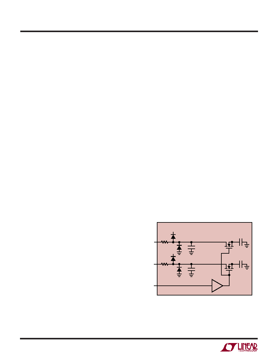
Figure 2 shows an equivalent circuit for the LTC2229
CMOS differential sample-and-hold. The analog inputs are
connected to the sampling capacitors (CSAMPLE) through
NMOS transistors. The capacitors shown attached to each
input (CPARASITIC) are the summation of all other capaci-
tance associated with each input.
During the sample phase when CLK is low, the transistors
connect the analog inputs to the sampling capacitors and
they charge to and track the differential input voltage.
When CLK transitions from low to high, the sampled input
voltage is held on the sampling capacitors. During the hold
phase when CLK is high, the sampling capacitors are
disconnected from the input and the held voltage is passed
to the ADC core for processing. As CLK transitions from
high to low, the inputs are reconnected to the sampling
capacitors to acquire a new sample. Since the sampling
capacitors still hold the previous sample, a charging glitch
proportional to the change in voltage between samples will
be seen at this time. If the change between the last sample
and the new sample is small, the charging glitch seen at
the input will be small. If the input change is large, such as
the change seen with input frequencies near Nyquist, then
a larger charging glitch will be seen.
Figure 2. Equivalent Input Circuit
APPLICATIO S I FOR ATIO
WU
UU
VDD
15
15
CPARASITIC
1pF
CPARASITIC
1pF
CSAMPLE
4pF
CSAMPLE
4pF
LTC2229
AIN+
AIN–
CLK
2229 F02
相关PDF资料 |
PDF描述 |
|---|---|
| LTC2231IUP#TRPBF | IC ADC 10BIT 135MSPS 64-QFN |
| LTC2233CUK#TRPBF | IC ADC 10BIT 80MSPS SAMPL 48QFN |
| LTC2234IUK#TRPBF | IC ADC 10BIT 135MSPS SAMPL 48QFN |
| LTC2237IUH#TRPBF | IC ADC 10BIT 40MSPS 3V 32-QFN |
| LTC2239CUH#PBF | IC ADC 10-BIT 80MSPS 3V 32-QFN |
相关代理商/技术参数 |
参数描述 |
|---|---|
| LTC222CJ | 制造商:LINER 制造商全称:Linear Technology 功能描述:Micropower, Low Charge Injection, Quad CMOS Analog Switches with Data Latches |
| LTC222CN | 功能描述:IC SWITCH QUAD SPST 16DIP RoHS:否 类别:集成电路 (IC) >> 接口 - 模拟开关,多路复用器,多路分解器 系列:- 标准包装:1,000 系列:- 功能:多路复用器 电路:1 x 4:1 导通状态电阻:- 电压电源:双电源 电压 - 电源,单路/双路(±):±5V 电流 - 电源:7mA 工作温度:-40°C ~ 85°C 安装类型:表面贴装 封装/外壳:16-SOIC(0.154",3.90mm 宽) 供应商设备封装:16-SOIC 包装:带卷 (TR) |
| LTC222CN#PBF | 功能描述:IC SWITCH QUAD SPST 16DIP RoHS:是 类别:集成电路 (IC) >> 接口 - 模拟开关,多路复用器,多路分解器 系列:- 标准包装:48 系列:- 功能:开关 电路:4 x SPST - NO 导通状态电阻:100 欧姆 电压电源:单/双电源 电压 - 电源,单路/双路(±):2 V ~ 12 V,±2 V ~ 6 V 电流 - 电源:50nA 工作温度:-40°C ~ 85°C 安装类型:表面贴装 封装/外壳:16-SOIC(0.154",3.90mm 宽) 供应商设备封装:16-SOIC 包装:管件 |
| LTC222CS | 功能描述:IC SWITCH QUAD SPST 16SOIC RoHS:否 类别:集成电路 (IC) >> 接口 - 模拟开关,多路复用器,多路分解器 系列:- 标准包装:1,000 系列:- 功能:多路复用器 电路:1 x 4:1 导通状态电阻:- 电压电源:双电源 电压 - 电源,单路/双路(±):±5V 电流 - 电源:7mA 工作温度:-40°C ~ 85°C 安装类型:表面贴装 封装/外壳:16-SOIC(0.154",3.90mm 宽) 供应商设备封装:16-SOIC 包装:带卷 (TR) |
| LTC222CS#PBF | 功能描述:IC SWITCH QUAD SPST 16SOIC RoHS:是 类别:集成电路 (IC) >> 接口 - 模拟开关,多路复用器,多路分解器 系列:- 标准包装:1,000 系列:- 功能:多路复用器 电路:1 x 4:1 导通状态电阻:- 电压电源:双电源 电压 - 电源,单路/双路(±):±5V 电流 - 电源:7mA 工作温度:-40°C ~ 85°C 安装类型:表面贴装 封装/外壳:16-SOIC(0.154",3.90mm 宽) 供应商设备封装:16-SOIC 包装:带卷 (TR) |
发布紧急采购,3分钟左右您将得到回复。