- 您现在的位置:买卖IC网 > PDF目录10661 > LTC2245IUH#PBF (Linear Technology)IC ADC 14-BIT 10MSPS 3V 32-QFN PDF资料下载
参数资料
| 型号: | LTC2245IUH#PBF |
| 厂商: | Linear Technology |
| 文件页数: | 18/20页 |
| 文件大小: | 0K |
| 描述: | IC ADC 14-BIT 10MSPS 3V 32-QFN |
| 标准包装: | 73 |
| 位数: | 14 |
| 采样率(每秒): | 10M |
| 数据接口: | 并联 |
| 转换器数目: | 1 |
| 功率耗散(最大): | 69mW |
| 电压电源: | 单电源 |
| 工作温度: | -40°C ~ 85°C |
| 安装类型: | 表面贴装 |
| 封装/外壳: | 32-WFQFN 裸露焊盘 |
| 供应商设备封装: | 32-QFN 裸露焊盘(5x5) |
| 包装: | 管件 |
| 输入数目和类型: | 1 个单端,双极; 1 个差分,双极 |
| 产品目录页面: | 1349 (CN2011-ZH PDF) |
LTC2245
7
2245fa
TYPICAL PERFOR A CE CHARACTERISTICS
UW
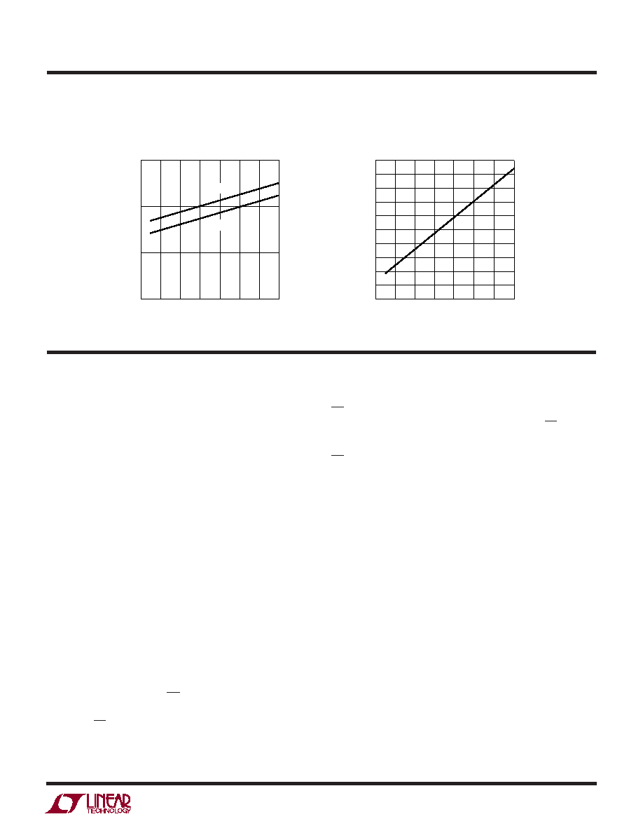
IOVDD vs Sample Rate, 5MHz Sine
Wave Input, –1dB, OVDD = 1.8V
IVDD vs Sample Rate,
5MHz Sine Wave Input, –1dB
UU
U
PI FU CTIO S
AIN+ (Pin 1): Positive Differential Analog Input.
AIN- (Pin 2): Negative Differential Analog Input.
REFH (Pins 3, 4): ADC High Reference. Short together and
bypass to pins 5, 6 with a 0.1
F ceramic chip capacitor as
close to the pin as possible. Also bypass to pins 5, 6 with
an additional 2.2
F ceramic chip capacitor and to ground
with a 1
F ceramic chip capacitor.
REFL (Pins 5, 6): ADC Low Reference. Short together and
bypass to pins 3, 4 with a 0.1
F ceramic chip capacitor as
close to the pin as possible. Also bypass to pins 3, 4 with
an additional 2.2
F ceramic chip capacitor and to ground
with a 1
F ceramic chip capacitor.
VDD (Pins 7, 32): 3V Supply. Bypass to GND with 0.1F
ceramic chip capacitors.
GND (Pin 8): ADC Power Ground.
CLK (Pin 9): Clock Input. The input sample starts on the
positive edge.
SHDN (Pin 10): Shutdown Mode Selection Pin. Connect-
ing SHDN to GND and OE to GND results in normal
operation with the outputs enabled. Connecting SHDN to
GND and OE to VDD results in normal operation with the
outputs at high impedance. Connecting SHDN to VDD and
OE to GND results in nap mode with the outputs at high
impedance. Connecting SHDN to VDD and OE to VDD
results in sleep mode with the outputs at high impedance.
OE (Pin 11): Output Enable Pin. Refer to SHDN pin
function.
D0 – D13 (Pins 12, 13, 14, 15, 16, 17, 18, 19, 22, 23, 24,
25, 26, 27): Digital Outputs. D13 is the MSB.
OGND (Pin 20): Output Driver Ground.
OVDD (Pin 21): Positive Supply for the Output Drivers.
Bypass to ground with 0.1
F ceramic chip capacitor.
OF (Pin 28): Over/Under Flow Output. High when an over
or under flow has occurred.
MODE (Pin 29): Output Format and Clock Duty Cycle
Stabilizer Selection Pin. Connecting MODE to GND selects
offset binary output format and turns the clock duty cycle
stabilizer off. 1/3 VDD selects offset binary output format
and turns the clock duty cycle stabilizer on. 2/3 VDD selects
2’s complement output format and turns the clock duty
cycle stabilizer on. VDD selects 2’s complement output
format and turns the clock duty cycle stabilizer off.
SAMPLE RATE (Msps)
10
I VDD
(mA)
15
20
25
02468
2245 G12
10
12
14
2V RANGE
1V RANGE
SAMPLE RATE (Msps)
0
I OVDD
(mA)
0.1
0.3
0.4
0.5
1.0
0.7
4
8
10
2245 G13
0.2
0.8
0.9
0.6
2
6
12
14
相关PDF资料 |
PDF描述 |
|---|---|
| MAX917ESA+ | IC COMPARATOR BTR 8-SOIC |
| AD9225ARSZ | IC ADC 12BIT 25MSPS 28-SSOP |
| VI-B1W-IV-F1 | CONVERTER MOD DC/DC 5.5V 150W |
| AD9225ARZ | IC ADC 12BIT 25MSPS 28-SOIC |
| VE-B1W-IV-F2 | CONVERTER MOD DC/DC 5.5V 150W |
相关代理商/技术参数 |
参数描述 |
|---|---|
| LTC2246 | 制造商:LINER 制造商全称:Linear Technology 功能描述:14-Bit, 80Msps Low Power 3V ADC |
| LTC2246CUH | 制造商:Linear Technology 功能描述:ADC Single Pipelined 25Msps 14-bit Parallel 32-Pin QFN EP |
| LTC2246CUH#PBF | 功能描述:IC ADC 14BIT 25MSPS SAMPL 32-QFN RoHS:是 类别:集成电路 (IC) >> 数据采集 - 模数转换器 系列:- 标准包装:1 系列:microPOWER™ 位数:8 采样率(每秒):1M 数据接口:串行,SPI? 转换器数目:1 功率耗散(最大):- 电压电源:模拟和数字 工作温度:-40°C ~ 125°C 安装类型:表面贴装 封装/外壳:24-VFQFN 裸露焊盘 供应商设备封装:24-VQFN 裸露焊盘(4x4) 包装:Digi-Reel® 输入数目和类型:8 个单端,单极 产品目录页面:892 (CN2011-ZH PDF) 其它名称:296-25851-6 |
| LTC2246CUH#PBF | 制造商:Linear Technology 功能描述:IC, ADC, 14BIT, 25MSPS, QFN-32 |
| LTC2246CUH#TRPBF | 功能描述:IC ADC 14BIT 25MSPS SAMPL 32-QFN RoHS:是 类别:集成电路 (IC) >> 数据采集 - 模数转换器 系列:- 标准包装:1,000 系列:- 位数:12 采样率(每秒):300k 数据接口:并联 转换器数目:1 功率耗散(最大):75mW 电压电源:单电源 工作温度:0°C ~ 70°C 安装类型:表面贴装 封装/外壳:24-SOIC(0.295",7.50mm 宽) 供应商设备封装:24-SOIC 包装:带卷 (TR) 输入数目和类型:1 个单端,单极;1 个单端,双极 |
发布紧急采购,3分钟左右您将得到回复。