- 您现在的位置:买卖IC网 > PDF目录10661 > LTC2246CUH#PBF (Linear Technology)IC ADC 14BIT 25MSPS SAMPL 32-QFN PDF资料下载
参数资料
| 型号: | LTC2246CUH#PBF |
| 厂商: | Linear Technology |
| 文件页数: | 10/24页 |
| 文件大小: | 0K |
| 描述: | IC ADC 14BIT 25MSPS SAMPL 32-QFN |
| 标准包装: | 73 |
| 位数: | 14 |
| 采样率(每秒): | 25M |
| 数据接口: | 并联 |
| 转换器数目: | 1 |
| 功率耗散(最大): | 90mW |
| 电压电源: | 单电源 |
| 工作温度: | 0°C ~ 70°C |
| 安装类型: | 表面贴装 |
| 封装/外壳: | 32-WFQFN 裸露焊盘 |
| 供应商设备封装: | 32-QFN 裸露焊盘(5x5) |
| 包装: | 管件 |
| 输入数目和类型: | 1 个单端,双极; 1 个差分,双极 |
LTC2248/LTC2247/LTC2246
18
224876fa
APPLICATIO S I FOR ATIO
WU
UU
bearing on how much SNR degradation will be experi-
enced. For high crest factor signals such as WCDMA or
OFDM, where the nominal power level must be at least 6dB
to 8dB below full scale, the use of these translators will
have a lesser impact.
The transformer in the example may be terminated with
the appropriate termination for the signaling in use. The
use of a transformer with a 1:4 impedance ratio may be
desirable in cases where lower voltage differential signals
are considered. The center tap may be bypassed to ground
through a capacitor close to the ADC if the differential
signals originate on a different plane. The use of a capaci-
tor at the input may result in peaking, and depending on
transmission line length may require a 10
to 20 ohm
series resistor to act as both a low pass filter for high
frequency noise that may be induced into the clock line by
neighboring digital signals, as well as a damping mecha-
nism for reflections.
Maximum and Minimum Conversion Rates
The maximum conversion rate for the LTC2248/LTC2247/
LTC2246 is 65Msps (LTC2248), 40Msps (LTC2247), and
25Msps (LTC2246). For the ADC to operate properly, the
CLK signal should have a 50% (
±5%) duty cycle. Each half
cycle must have at least 7.3ns (LTC2248), 11.8ns
(LTC2247), and 18.9ns (LTC2246) for the ADC internal
circuitry to have enough settling time for proper operation.
An optional clock duty cycle stabilizer circuit can be used
if the input clock has a non 50% duty cycle. This circuit
uses the rising edge of the CLK pin to sample the analog
input. The falling edge of CLK is ignored and the internal
falling edge is generated by a phase-locked loop. The input
clock duty cycle can vary from 40% to 60% and the clock
duty cycle stabilizer will maintain a constant 50% internal
duty cycle. If the clock is turned off for a long period of
time, the duty cycle stabilizer circuit will require a hundred
clock cycles for the PLL to lock onto the input clock. To use
the clock duty cycle stabilizer, the MODE pin should be
connected to 1/3VDD or 2/3VDD using external resistors.
The lower limit of the LTC2248/LTC2247/LTC2246 sample
rate is determined by droop of the sample-and-hold cir-
cuits. The pipelined architecture of this ADC relies on
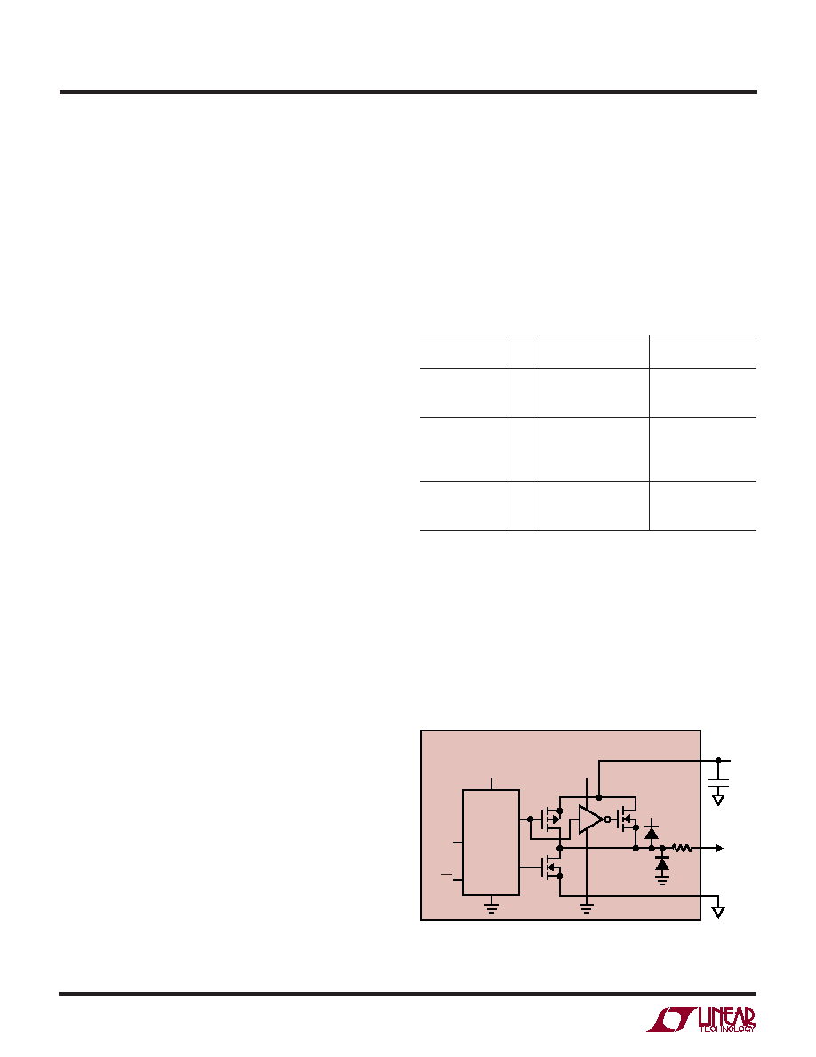
Figure 14. Digital Output Buffer
LTC2248/47/46
224876 F12
OVDD
VDD
0.1
F
43
TYPICAL
DATA
OUTPUT
OGND
OVDD
0.5V
TO 3.6V
PREDRIVER
LOGIC
DATA
FROM
LATCH
OE
Table 1. Output Codes vs Input Voltage
AIN+ – AIN–
D13 – D0
(2V Range)
OF
(Offset Binary)
(2’s Complement)
>+1.000000V
1
11 1111 1111 1111
01 1111 1111 1111
+0.999878V
0
11 1111 1111 1111
01 1111 1111 1111
+0.999756V
0
11 1111 1111 1110
01 1111 1111 1110
+0.000122V
0
10 0000 0000 0001
00 0000 0000 0001
0.000000V
0
10 0000 0000 0000
00 0000 0000 0000
–0.000122V
0
01 1111 1111 1111
11 1111 1111 1111
–0.000244V
0
01 1111 1111 1110
11 1111 1111 1110
–0.999878V
0
00 0000 0000 0001
10 0000 0000 0001
–1.000000V
0
00 0000 0000 0000
10 0000 0000 0000
<–1.000000V
1
00 0000 0000 0000
10 0000 0000 0000
storing analog signals on small valued capacitors. Junc-
tion leakage will discharge the capacitors. The specified
minimum operating frequency for the LTC2248/LTC2247/
LTC2246 is 1Msps.
DIGITAL OUTPUTS
Table 1 shows the relationship between the analog input
voltage, the digital data bits, and the overflow bit.
Digital Output Buffers
Figure 14 shows an equivalent circuit for a single output
buffer. Each buffer is powered by OVDD and OGND, iso-
lated from the ADC power and ground. The additional
N-channel transistor in the output driver allows operation
down to low voltages. The internal resistor in series with
the output makes the output appear as 50
to external
circuitry and may eliminate the need for external damping
resistors.
相关PDF资料 |
PDF描述 |
|---|---|
| VE-B1W-IV-F4 | CONVERTER MOD DC/DC 5.5V 150W |
| VE-B1X-IV-F3 | CONVERTER MOD DC/DC 5.2V 150W |
| MAX917ESA+T | IC COMPARATOR BTR 8-SOIC |
| LTC2228CUH#PBF | IC ADC 12BIT 65MSPS SAMPL 32-QFN |
| MAX992EKA+T | IC COMPARATOR R-R SOT23-8 |
相关代理商/技术参数 |
参数描述 |
|---|---|
| LTC2246H | 制造商:LINER 制造商全称:Linear Technology 功能描述:14-Bit, 25Msps 125°C ADC In LQFP |
| LTC2246HLU#PBF | 功能描述:IC ADC 14BIT 25MSPS 32-TQFP RoHS:是 类别:集成电路 (IC) >> 数据采集 - 模数转换器 系列:- 产品培训模块:Lead (SnPb) Finish for COTS Obsolescence Mitigation Program 标准包装:2,500 系列:- 位数:12 采样率(每秒):3M 数据接口:- 转换器数目:- 功率耗散(最大):- 电压电源:- 工作温度:- 安装类型:表面贴装 封装/外壳:SOT-23-6 供应商设备封装:SOT-23-6 包装:带卷 (TR) 输入数目和类型:- |
| LTC2246HLX | 制造商:LINER 制造商全称:Linear Technology 功能描述:14-Bit, 25Msps 125°C ADC In LQFP |
| LTC2246HLX#PBF | 功能描述:IC ADC 14BIT 25MSPS 48-LQFP RoHS:是 类别:集成电路 (IC) >> 数据采集 - 模数转换器 系列:- 标准包装:1 系列:- 位数:14 采样率(每秒):83k 数据接口:串行,并联 转换器数目:1 功率耗散(最大):95mW 电压电源:双 ± 工作温度:0°C ~ 70°C 安装类型:通孔 封装/外壳:28-DIP(0.600",15.24mm) 供应商设备封装:28-PDIP 包装:管件 输入数目和类型:1 个单端,双极 |
| LTC2246HLX-PBF | 制造商:LINER 制造商全称:Linear Technology 功能描述:14-Bit, 25Msps 125°C ADC In LQFP |
发布紧急采购,3分钟左右您将得到回复。