- 您现在的位置:买卖IC网 > PDF目录2005 > LTC2249IUH#TRPBF (Linear Technology)IC ADC 14BIT 80MSPS LP 32-QFN PDF资料下载
参数资料
| 型号: | LTC2249IUH#TRPBF |
| 厂商: | Linear Technology |
| 文件页数: | 8/24页 |
| 文件大小: | 0K |
| 描述: | IC ADC 14BIT 80MSPS LP 32-QFN |
| 标准包装: | 2,500 |
| 位数: | 14 |
| 采样率(每秒): | 80M |
| 数据接口: | 并联 |
| 转换器数目: | 1 |
| 功率耗散(最大): | 258mW |
| 电压电源: | 单电源 |
| 工作温度: | -40°C ~ 85°C |
| 安装类型: | 表面贴装 |
| 封装/外壳: | 32-WFQFN 裸露焊盘 |
| 供应商设备封装: | 32-QFN 裸露焊盘(5x5) |
| 包装: | 带卷 (TR) |
| 输入数目和类型: | 1 个单端,双极; 1 个差分,双极 |
LTC2249
16
2249fa
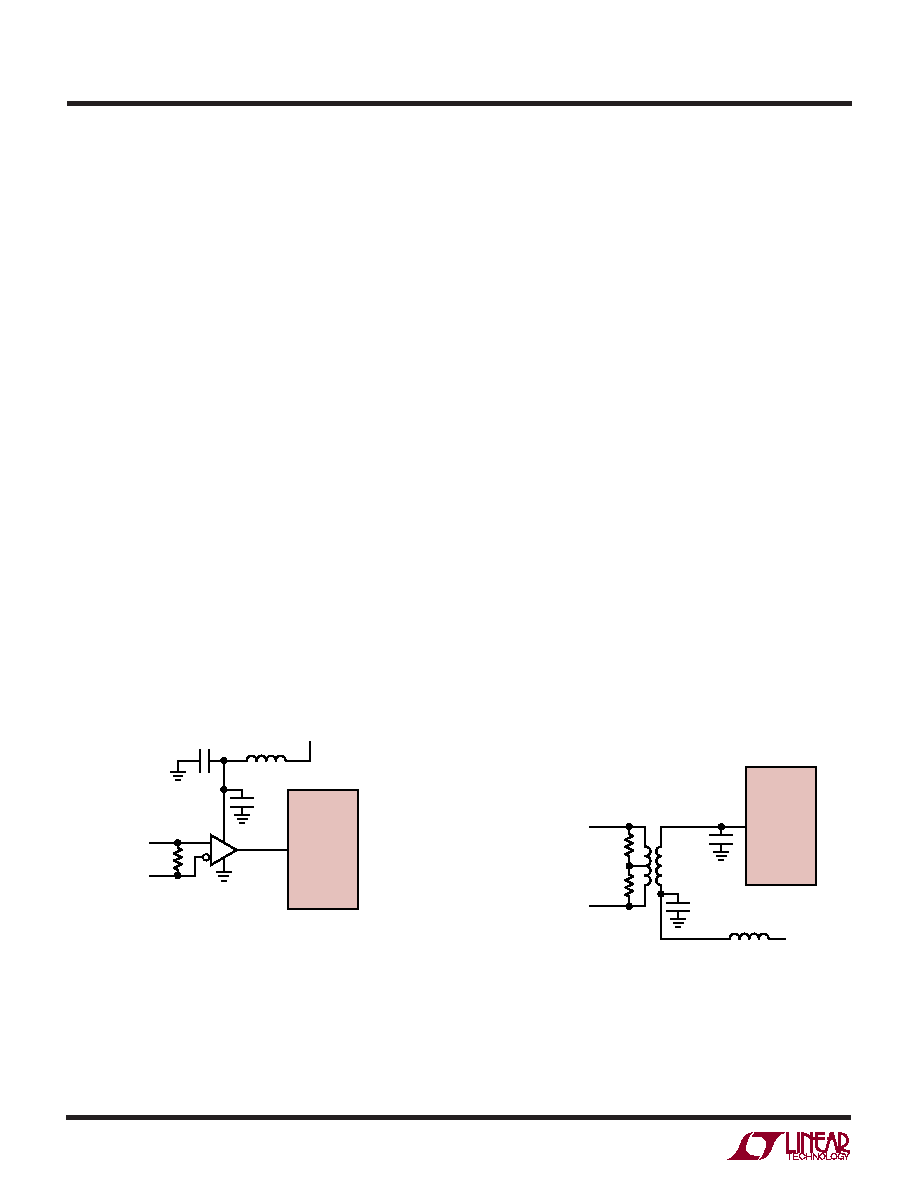
Figures 12 and 13 show alternatives for converting a
differential clock to the single-ended CLK input. The use of
a transformer provides no incremental contribution to
phase noise. The LVDS or PECL to CMOS translators
provide little degradation below 70MHz, but at 140MHz
will degrade the SNR compared to the transformer solu-
tion. The nature of the received signals also has a large
bearing on how much SNR degradation will be experi-
enced. For high crest factor signals such as WCDMA or
OFDM, where the nominal power level must be at least 6dB
to 8dB below full scale, the use of these translators will
have a lesser impact.
The transformer in the example may be terminated with
the appropriate termination for the signaling in use. The
use of a transformer with a 1:4 impedance ratio may be
desirable in cases where lower voltage differential signals
are considered. The center tap may be bypassed to ground
through a capacitor close to the ADC if the differential
signals originate on a different plane. The use of a capaci-
tor at the input may result in peaking, and depending on
transmission line length may require a 10
to 20 ohm
series resistor to act as both a low pass filter for high
frequency noise that may be induced into the clock line by
neighboring digital signals, as well as a damping mecha-
nism for reflections.
Maximum and Minimum Conversion Rates
The maximum conversion rate for the LTC2249 is 80Msps.
For the ADC to operate properly, the CLK signal should
have a 50% (
±5%) duty cycle. Each half cycle must have
at least 5.9ns for the ADC internal circuitry to have enough
settling time for proper operation.
An optional clock duty cycle stabilizer circuit can be used
if the input clock has a non 50% duty cycle. This circuit
uses the rising edge of the CLK pin to sample the analog
input. The falling edge of CLK is ignored and the internal
falling edge is generated by a phase-locked loop. The input
clock duty cycle can vary from 40% to 60% and the clock
duty cycle stabilizer will maintain a constant 50% internal
duty cycle. If the clock is turned off for a long period of
time, the duty cycle stabilizer circuit will require a hundred
clock cycles for the PLL to lock onto the input clock. To use
the clock duty cycle stabilizer, the MODE pin should be
connected to 1/3VDD or 2/3VDD using external resistors.
The lower limit of the LTC2249 sample rate is determined
by droop of the sample-and-hold circuits. The pipelined
architecture of this ADC relies on storing analog signals on
small valued capacitors. Junction leakage will discharge
the capacitors. The specified minimum operating fre-
quency for the LTC2249 is 1Msps.
APPLICATIO S I FOR ATIO
WU
UU
Figure 13. LVDS or PECL CLK Drive Using a Transformer
Figure 12. CLK Drive Using an LVDS or PECL to CMOS Converter
CLK
100
0.1
F
4.7
F
FERRITE
BEAD
CLEAN
SUPPLY
IF LVDS USE FIN1002 OR FIN1018.
FOR PECL, USE AZ1000ELT21 OR SIMILAR
2249 F12
LTC2249
CLK
5pF-30pF
ETC1-1T
0.1
F
VCM
FERRITE
BEAD
DIFFERENTIAL
CLOCK
INPUT
2249 F13
LTC2249
相关PDF资料 |
PDF描述 |
|---|---|
| LTC2251IUH#PBF | IC ADC 10-BIT 125MSPS 3V 32-QFN |
| LTC2253IUH#TRPBF | IC ADC 12BIT 125MSPS 3V 32-QFN |
| LTC2255CUH#TRPBF | IC ADC 14BIT 125MSPS 3V 32-QFN |
| LTC2258IUJ-12#PBF | IC ADC 12BIT 65MSPS 1.8V 40-QFN |
| LTC2262CUJ-14#TRPBF | IC ADC 14BIT 150MSPS 40-QFN |
相关代理商/技术参数 |
参数描述 |
|---|---|
| LTC2250 | 制造商:LINER 制造商全称:Linear Technology 功能描述:10-Bit, 125/105Msps Low Noise 3V ADCs |
| LTC2250CUH | 制造商:Linear Technology 功能描述:ADC Single Pipelined 105Msps 10-bit Parallel 32-Pin QFN EP |
| LTC2250CUH#PBF | 功能描述:IC ADC 10-BIT 105MSPS 3V 32-QFN RoHS:是 类别:集成电路 (IC) >> 数据采集 - 模数转换器 系列:- 标准包装:1,000 系列:- 位数:12 采样率(每秒):300k 数据接口:并联 转换器数目:1 功率耗散(最大):75mW 电压电源:单电源 工作温度:0°C ~ 70°C 安装类型:表面贴装 封装/外壳:24-SOIC(0.295",7.50mm 宽) 供应商设备封装:24-SOIC 包装:带卷 (TR) 输入数目和类型:1 个单端,单极;1 个单端,双极 |
| LTC2250CUH#PBF | 制造商:Linear Technology 功能描述:A/D Converter (A-D) IC |
| LTC2250CUH#TRPBF | 功能描述:IC ADC 10BIT 105MSPS 3V 32-QFN RoHS:是 类别:集成电路 (IC) >> 数据采集 - 模数转换器 系列:- 标准包装:1,000 系列:- 位数:16 采样率(每秒):45k 数据接口:串行 转换器数目:2 功率耗散(最大):315mW 电压电源:模拟和数字 工作温度:0°C ~ 70°C 安装类型:表面贴装 封装/外壳:28-SOIC(0.295",7.50mm 宽) 供应商设备封装:28-SOIC W 包装:带卷 (TR) 输入数目和类型:2 个单端,单极 |
发布紧急采购,3分钟左右您将得到回复。