- 您现在的位置:买卖IC网 > PDF目录10654 > LTC2252IUH#PBF (Linear Technology)IC ADC 12-BIT 105MSPS 3V 32-QFN PDF资料下载
参数资料
| 型号: | LTC2252IUH#PBF |
| 厂商: | Linear Technology |
| 文件页数: | 5/24页 |
| 文件大小: | 0K |
| 描述: | IC ADC 12-BIT 105MSPS 3V 32-QFN |
| 标准包装: | 73 |
| 位数: | 12 |
| 采样率(每秒): | 105M |
| 数据接口: | 并联 |
| 转换器数目: | 1 |
| 功率耗散(最大): | 378mW |
| 电压电源: | 单电源 |
| 工作温度: | -40°C ~ 85°C |
| 安装类型: | 表面贴装 |
| 封装/外壳: | 32-WFQFN 裸露焊盘 |
| 供应商设备封装: | 32-QFN 裸露焊盘(5x5) |
| 包装: | 管件 |
| 输入数目和类型: | 1 个单端,双极; 1 个差分,双极 |
| 产品目录页面: | 1349 (CN2011-ZH PDF) |
LTC2253/LTC2252
13
22532fa
the quantized value is subtracted from the input by the
DAC to produce a residue. The residue is amplified and
output by the residue amplifier. Successive stages operate
out of phase so that when the odd stages are outputting
their residue, the even stages are acquiring that residue
and vice versa.
When CLK is low, the analog input is sampled differentially
directly onto the input sample-and-hold capacitors, inside
the “Input S/H” shown in the block diagram. At the instant
that CLK transitions from low to high, the sampled input is
held. While CLK is high, the held input voltage is buffered
by the S/H amplifier which drives the first pipelined ADC
stage. The first stage acquires the output of the S/H during
this high phase of CLK. When CLK goes back low, the first
stage produces its residue which is acquired by the
second stage. At the same time, the input S/H goes back
to acquiring the analog input. When CLK goes back high,
the second stage produces its residue which is acquired
by the third stage. An identical process is repeated for the
third, fourth and fifth stages, resulting in a fifth stage
residue that is sent to the sixth stage ADC for final
evaluation.
Each ADC stage following the first has additional range to
accommodate flash and amplifier offset errors. Results
from all of the ADC stages are digitally synchronized such
that the results can be properly combined in the correction
logic before being sent to the output buffer.
SAMPLE/HOLD OPERATION AND INPUT DRIVE
Sample/Hold Operation
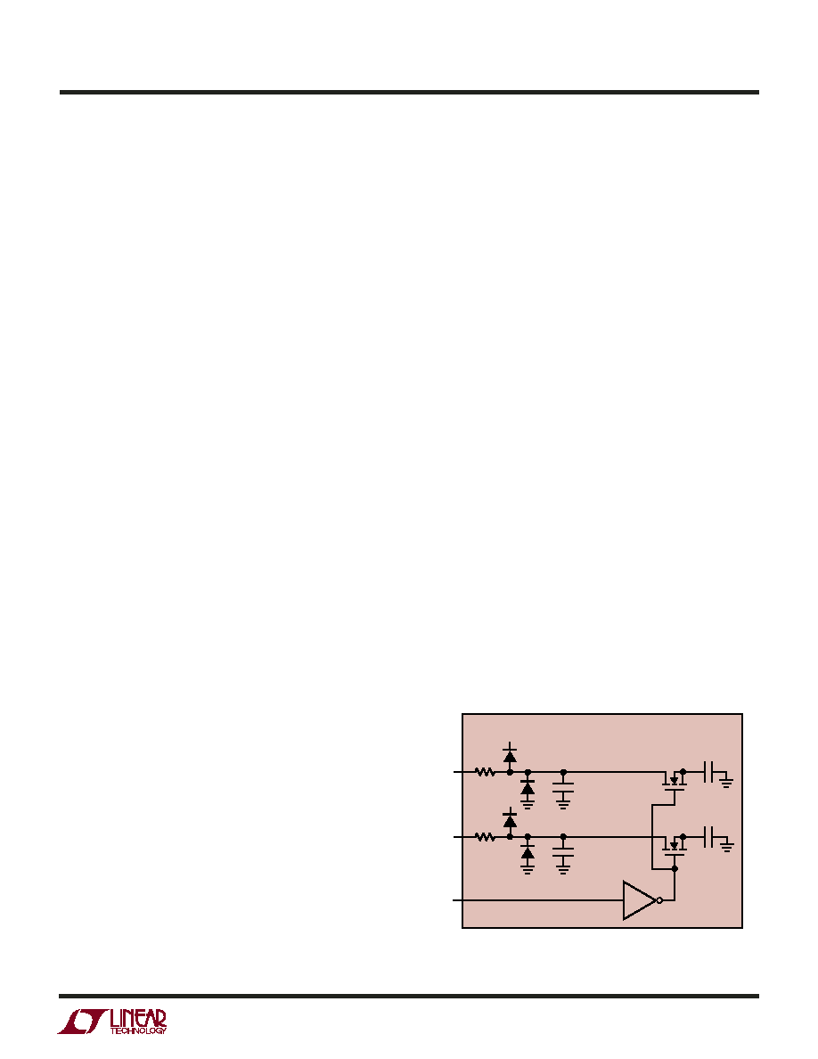
Figure 2 shows an equivalent circuit for the LTC2253/
LTC2252 CMOS differential sample-and-hold. The analog
inputs are connected to the sampling capacitors (CSAMPLE)
through NMOS transistors. The capacitors shown at-
tached to each input (CPARASITIC) are the summation of all
other capacitance associated with each input.
During the sample phase when CLK is low, the transistors
connect the analog inputs to the sampling capacitors and
they charge to and track the differential input voltage.
When CLK transitions from low to high, the sampled input
APPLICATIO S I FOR ATIO
WU
U
voltage is held on the sampling capacitors. During the hold
phase when CLK is high, the sampling capacitors are
disconnected from the input and the held voltage is passed
to the ADC core for processing. As CLK transitions from
high to low, the inputs are reconnected to the sampling
capacitors to acquire a new sample. Since the sampling
capacitors still hold the previous sample, a charging glitch
proportional to the change in voltage between samples will
be seen at this time. If the change between the last sample
and the new sample is small, the charging glitch seen at
the input will be small. If the input change is large, such as
the change seen with input frequencies near Nyquist, then
a larger charging glitch will be seen.
Single-Ended Input
For cost sensitive applications, the analog inputs can be
driven single-ended. With a single-ended input the har-
monic distortion and INL will degrade, but the SNR and
DNL will remain unchanged. For a single-ended input, AIN+
should be driven with the input signal and AIN– should be
connected to 1.5V or VCM.
Common Mode Bias
For optimal performance the analog inputs should be
driven differentially. Each input should swing
±0.5V for
the 2V range or
±0.25V for the 1V range, around a
common mode voltage of 1.5V. The VCM output pin (Pin
31) may be used to provide the common mode bias level.
VCM can be tied directly to the center tap of a transformer
VDD
15
15
CPARASITIC
1pF
CPARASITIC
1pF
CSAMPLE
3.5pF
CSAMPLE
3.5pF
LTC2253/LTC2252
AIN+
AIN–
CLK
22532 F02
Figure 2. Equivalent Input Circuit
相关PDF资料 |
PDF描述 |
|---|---|
| MAX995EUD+T | IC COMPARATOR R-R 14-TSSOP |
| VE-21R-IW-F3 | CONVERTER MOD DC/DC 7.5V 100W |
| MAX9112EKA+T | IC DVR LVDS DUAL SOT23-8 |
| LTC2253CUH#PBF | IC ADC 12-BIT 125MSPS 3V 32-QFN |
| VE-B1K-MX-F2 | CONVERTER MOD DC/DC 40V 75W |
相关代理商/技术参数 |
参数描述 |
|---|---|
| LTC2253 | 制造商:LINER 制造商全称:Linear Technology 功能描述:12-Bit, 125/105Msps Low Power 3V ADCs |
| LTC2253CUH | 制造商:LINER 制造商全称:Linear Technology 功能描述:12-Bit, 125/105Msps Low Power 3V ADCs |
| LTC2253CUH#PBF | 功能描述:IC ADC 12-BIT 125MSPS 3V 32-QFN RoHS:是 类别:集成电路 (IC) >> 数据采集 - 模数转换器 系列:- 标准包装:1 系列:microPOWER™ 位数:8 采样率(每秒):1M 数据接口:串行,SPI? 转换器数目:1 功率耗散(最大):- 电压电源:模拟和数字 工作温度:-40°C ~ 125°C 安装类型:表面贴装 封装/外壳:24-VFQFN 裸露焊盘 供应商设备封装:24-VQFN 裸露焊盘(4x4) 包装:Digi-Reel® 输入数目和类型:8 个单端,单极 产品目录页面:892 (CN2011-ZH PDF) 其它名称:296-25851-6 |
| LTC2253CUH#TRPBF | 功能描述:IC ADC 12BIT 125MSPS 3V 32-QFN RoHS:是 类别:集成电路 (IC) >> 数据采集 - 模数转换器 系列:- 标准包装:1 系列:- 位数:14 采样率(每秒):83k 数据接口:串行,并联 转换器数目:1 功率耗散(最大):95mW 电压电源:双 ± 工作温度:0°C ~ 70°C 安装类型:通孔 封装/外壳:28-DIP(0.600",15.24mm) 供应商设备封装:28-PDIP 包装:管件 输入数目和类型:1 个单端,双极 |
| LTC2253IUH | 制造商:Linear Technology 功能描述:ADC Single Pipelined 125Msps 12-bit Parallel 32-Pin QFN EP |
发布紧急采购,3分钟左右您将得到回复。