- 您现在的位置:买卖IC网 > PDF目录10062 > LTC2254CUH#TRPBF (Linear Technology)IC ADC 14BIT 105MSPS 3V 32-QFN PDF资料下载
参数资料
| 型号: | LTC2254CUH#TRPBF |
| 厂商: | Linear Technology |
| 文件页数: | 6/24页 |
| 文件大小: | 0K |
| 描述: | IC ADC 14BIT 105MSPS 3V 32-QFN |
| 标准包装: | 2,500 |
| 位数: | 14 |
| 采样率(每秒): | 105M |
| 数据接口: | 并联 |
| 转换器数目: | 1 |
| 功率耗散(最大): | 378mW |
| 电压电源: | 单电源 |
| 工作温度: | 0°C ~ 70°C |
| 安装类型: | 表面贴装 |
| 封装/外壳: | 32-WFQFN 裸露焊盘 |
| 供应商设备封装: | 32-QFN 裸露焊盘(5x5) |
| 包装: | 带卷 (TR) |
| 输入数目和类型: | 1 个单端,双极; 1 个差分,双极 |
LTC2255/LTC2254
14
22554fa
Input Drive Impedance
As with all high performance, high speed ADCs, the
dynamic performance of the LTC2255/LTC2254 can be
influenced by the input drive circuitry, particularly the
second and third harmonics. Source impedance and reac-
tance can influence SFDR. At the falling edge of CLK, the
sample-and-hold circuit will connect the 3.5pF sampling
capacitor to the input pin and start the sampling period.
The sampling period ends when CLK rises, holding the
sampled input on the sampling capacitor. Ideally the input
circuitry should be fast enough to fully charge
the sampling capacitor during the sampling period
1/(2FENCODE); however, this is not always possible and the
incomplete settling may degrade the SFDR. The sampling
glitch has been designed to be as linear as possible to
minimize the effects of incomplete settling.
For the best performance, it is recommended to have a
source impedance of 100
or less for each input. The
source impedance should be matched for the differential
inputs. Poor matching will result in higher even order
harmonics, especially the second.
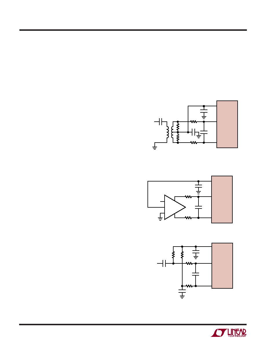
Input Drive Circuits
Figure 3 shows the LTC2255/LTC2254 being driven by an
RF transformer with a center tapped secondary. The
secondary center tap is DC biased with VCM, setting the
ADC input signal at its optimum DC level. Terminating on
the transformer secondary is desirable, as this provides a
common mode path for charging glitches caused by the
sample and hold. Figure 3 shows a 1:1 turns ratio trans-
former. Other turns ratios can be used if the source
impedance seen by the ADC does not exceed 100
for
each ADC input. A disadvantage of using a transformer is
the loss of low frequency response. Most small RF trans-
formers have poor performance at frequencies below
1MHz.
Figure 4 demonstrates the use of a differential amplifier to
convert a single ended input signal into a differential input
signal. The advantage of this method is that it provides low
frequency input response; however, the limited gain band-
width of most op amps will limit the SFDR at high input
frequencies.
APPLICATIO S I FOR ATIO
WU
UU
Figure 5. Single-Ended Drive
Figure 5 shows a single-ended input circuit. The imped-
ance seen by the analog inputs should be matched. This
circuit is not recommended if low distortion is required.
The 25
resistorsand12pFcapacitorontheanaloginputs
serve two purposes: isolating the drive circuitry from the
sample-and-hold charging glitches and limiting the
wideband noise at the converter input.
Figure 3. Single-Ended to Differential Conversion
Using a Transformer
Figure 4. Differential Drive with an Amplifier
25
25
25
25
0.1
F
AIN
+
AIN
–
12pF
2.2
F
VCM
LTC2255/
LTC2254
ANALOG
INPUT
0.1
FT1
1:1
T1 = MA/COM ETC1-1T
RESISTORS, CAPACITORS
ARE 0402 PACKAGE SIZE
22554 F03
25
25
12pF
2.2
F
VCM
LTC2255/
LTC2254
22554 F04
–
+
CM
ANALOG
INPUT
HIGH SPEED
DIFFERENTIAL
AMPLIFIER
AIN
+
AIN
–
25
0.1
F
ANALOG
INPUT
VCM
AIN
+
AIN
–
1k
12pF
224876 F05
2.2
F
1k
25
0.1
F
LTC2255/
LTC2254
相关PDF资料 |
PDF描述 |
|---|---|
| MS27466T23F53PC | CONN RCPT 53POS WALL MT W/PINS |
| VE-J7N-MX-S | CONVERTER MOD DC/DC 18.5V 75W |
| VE-J7L-MX-S | CONVERTER MOD DC/DC 28V 75W |
| VI-B6K-MW-F4 | CONVERTER MOD DC/DC 40V 100W |
| VE-BVY-MX | CONVERTER MOD DC/DC 3.3V 49.5W |
相关代理商/技术参数 |
参数描述 |
|---|---|
| LTC2254IUH | 制造商:Linear Technology 功能描述:ADC Single Pipelined 105Msps 14-bit Parallel 32-Pin QFN EP |
| LTC2254IUH#PBF | 功能描述:IC ADC 14-BIT 105MSPS 3V 32-QFN RoHS:是 类别:集成电路 (IC) >> 数据采集 - 模数转换器 系列:- 其它有关文件:TSA1204 View All Specifications 标准包装:1 系列:- 位数:12 采样率(每秒):20M 数据接口:并联 转换器数目:2 功率耗散(最大):155mW 电压电源:模拟和数字 工作温度:-40°C ~ 85°C 安装类型:表面贴装 封装/外壳:48-TQFP 供应商设备封装:48-TQFP(7x7) 包装:Digi-Reel® 输入数目和类型:4 个单端,单极;2 个差分,单极 产品目录页面:1156 (CN2011-ZH PDF) 其它名称:497-5435-6 |
| LTC2254IUH#TRPBF | 功能描述:IC ADC 14BIT 105MSPS 3V 32-QFN RoHS:是 类别:集成电路 (IC) >> 数据采集 - 模数转换器 系列:- 标准包装:1 系列:- 位数:14 采样率(每秒):83k 数据接口:串行,并联 转换器数目:1 功率耗散(最大):95mW 电压电源:双 ± 工作温度:0°C ~ 70°C 安装类型:通孔 封装/外壳:28-DIP(0.600",15.24mm) 供应商设备封装:28-PDIP 包装:管件 输入数目和类型:1 个单端,双极 |
| LTC2255 | 制造商:LINER 制造商全称:Linear Technology 功能描述:14-Bit, 125/105Msps Low Power 3V ADCs |
| LTC2255CUH | 制造商:Linear Technology 功能描述:ADC Single Pipelined 125Msps 14-bit Parallel 32-Pin QFN EP |
发布紧急采购,3分钟左右您将得到回复。