- 您现在的位置:买卖IC网 > PDF目录39415 > LTC2256CUJ-12#TRPBF (LINEAR TECHNOLOGY CORP) 1-CH 12-BIT PROPRIETARY METHOD ADC, PARALLEL ACCESS, PQCC40 PDF资料下载
参数资料
| 型号: | LTC2256CUJ-12#TRPBF |
| 厂商: | LINEAR TECHNOLOGY CORP |
| 元件分类: | ADC |
| 英文描述: | 1-CH 12-BIT PROPRIETARY METHOD ADC, PARALLEL ACCESS, PQCC40 |
| 封装: | 6 X 6 MM, LEAD FREE, PLASTIC, QFN-40 |
| 文件页数: | 16/32页 |
| 文件大小: | 1156K |
| 代理商: | LTC2256CUJ-12#TRPBF |
第1页第2页第3页第4页第5页第6页第7页第8页第9页第10页第11页第12页第13页第14页第15页当前第16页第17页第18页第19页第20页第21页第22页第23页第24页第25页第26页第27页第28页第29页第30页第31页第32页
LTC2258-12
LTC2257-12/LTC2256-12
23
225812fa
inductive coupling or coupling through the ground plane.
Even a tiny coupling factor can cause unwanted tones
in the ADC output spectrum. By randomizing the digital
output before it is transmitted off chip, these unwanted
tones can be randomized which reduces the unwanted
tone amplitude.
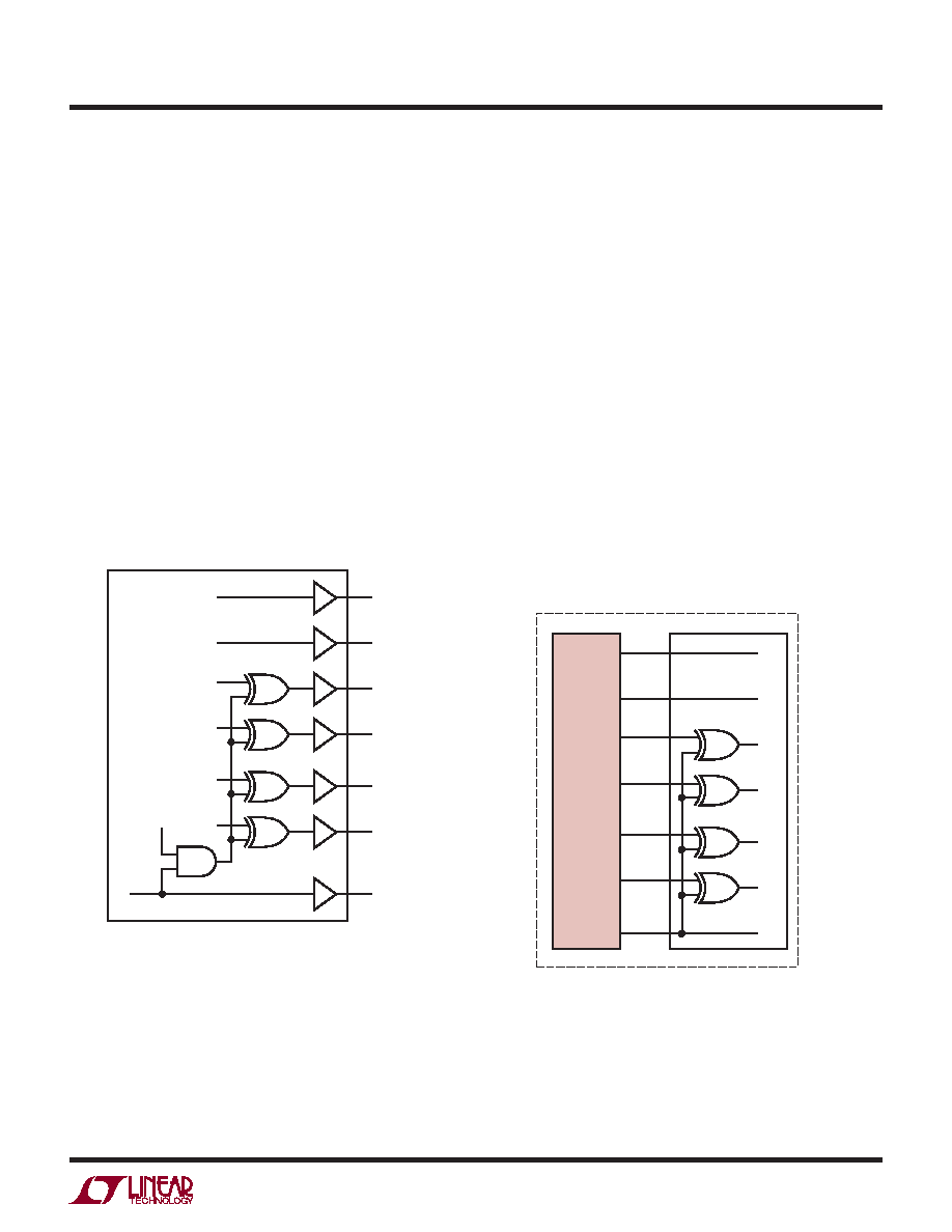
The digital output is “randomized” by applying an exclu-
sive-OR logic operation between the LSB and all other
data output bits. To decode, the reverse operation is ap-
plied—an exclusive-OR operation is applied between the
LSB and all other bits. The LSB, OF and CLKOUT outputs
are not affected. The output randomizer is enabled by
serially programming mode control register A4.
Alternate Bit Polarity
Another feature that reduces digital feedback on the circuit
board is the alternate bit polarity mode. When this mode
is enabled, all of the odd bits (D1, D3, D5, D7, D9, D11)
are inverted before the output buffers. The even bits (D0,
D2, D4, D6, D8, D10), OF and CLKOUT are not affected.
This can reduce digital currents in the circuit board ground
plane and reduce digital noise, particularly for very small
analog input signals.
When there is a very small signal at the input of the A/D
that is centered around midscale, the digital outputs toggle
between mostly 1s and mostly 0s. This simultaneous
switching of most of the bits will cause large currents in
the ground plane. By inverting every other bit, the alter-
nate bit polarity mode makes half of the bits transition
high while half of the bits transition low. To rst order,
this cancels current ow in the ground plane, reducing
the digital noise.
The digital output is decoded at the receiver by inverting
the odd bits (D1, D3, D5, D7, D9, D11). The alternate bit
polarity mode is independent of the digital output random-
APPLICATIONS INFORMATION
CLKOUT
OF
D11/D0
D10/D0
D2/D0
D1/D0
D0
225812 F15
OF
D11
D10
D2
D1
D0
RANDOMIZER
ON
D11
FPGA
PC BOARD
D10
D2
D1
D0
225812 F15
D0
D1/D0
D2/D0
D10/D0
D11/D0
OF
CLKOUT
LTC2258-12
Figure 15. Functional Equivalent of Digital Output Randomizer
Figure 16. Unrandomizing a Randomized Digital
Output Signal
相关PDF资料 |
PDF描述 |
|---|---|
| LTC2256IUJ-12#PBF | 1-CH 12-BIT PROPRIETARY METHOD ADC, PARALLEL ACCESS, PQCC40 |
| LTC2258CUJ-12#TRPBF | 1-CH 12-BIT PROPRIETARY METHOD ADC, PARALLEL ACCESS, PQCC40 |
| LTC2257IUJ-12#PBF | 1-CH 12-BIT PROPRIETARY METHOD ADC, PARALLEL ACCESS, PQCC40 |
| LTC2258IUJ-12#TRPBF | 1-CH 12-BIT PROPRIETARY METHOD ADC, PARALLEL ACCESS, PQCC40 |
| LTC2256IUJ-12#TRPBF | 1-CH 12-BIT PROPRIETARY METHOD ADC, PARALLEL ACCESS, PQCC40 |
相关代理商/技术参数 |
参数描述 |
|---|---|
| LTC2256CUJ-14#PBF | 功能描述:IC ADC 14BIT 25MSPS 1.8V 40-QFN RoHS:是 类别:集成电路 (IC) >> 数据采集 - 模数转换器 系列:- 标准包装:1 系列:microPOWER™ 位数:8 采样率(每秒):1M 数据接口:串行,SPI? 转换器数目:1 功率耗散(最大):- 电压电源:模拟和数字 工作温度:-40°C ~ 125°C 安装类型:表面贴装 封装/外壳:24-VFQFN 裸露焊盘 供应商设备封装:24-VQFN 裸露焊盘(4x4) 包装:Digi-Reel® 输入数目和类型:8 个单端,单极 产品目录页面:892 (CN2011-ZH PDF) 其它名称:296-25851-6 |
| LTC2256CUJ-14#TRPBF | 功能描述:IC ADC 14BIT 25MSPS 1.8V 40-QFN RoHS:是 类别:集成电路 (IC) >> 数据采集 - 模数转换器 系列:- 标准包装:1,000 系列:- 位数:12 采样率(每秒):300k 数据接口:并联 转换器数目:1 功率耗散(最大):75mW 电压电源:单电源 工作温度:0°C ~ 70°C 安装类型:表面贴装 封装/外壳:24-SOIC(0.295",7.50mm 宽) 供应商设备封装:24-SOIC 包装:带卷 (TR) 输入数目和类型:1 个单端,单极;1 个单端,双极 |
| LTC2256CUJ-14-PBF | 制造商:LINER 制造商全称:Linear Technology 功能描述:14-Bit, 65/40/25Msps Ultralow Power 1.8V ADCs |
| LTC2256CUJ-14-TRPBF | 制造商:LINER 制造商全称:Linear Technology 功能描述:14-Bit, 65/40/25Msps Ultralow Power 1.8V ADCs |
| LTC2256IUJ-12#PBF | 功能描述:IC ADC 12BIT 25MSPS 1.8V 40-QFN RoHS:是 类别:集成电路 (IC) >> 数据采集 - 模数转换器 系列:- 标准包装:1,000 系列:- 位数:12 采样率(每秒):300k 数据接口:并联 转换器数目:1 功率耗散(最大):75mW 电压电源:单电源 工作温度:0°C ~ 70°C 安装类型:表面贴装 封装/外壳:24-SOIC(0.295",7.50mm 宽) 供应商设备封装:24-SOIC 包装:带卷 (TR) 输入数目和类型:1 个单端,单极;1 个单端,双极 |
发布紧急采购,3分钟左右您将得到回复。