- 您现在的位置:买卖IC网 > PDF目录2005 > LTC2264CUJ-12#PBF (Linear Technology)IC ADC 12BIT SER/PAR 40M 40-QFN PDF资料下载
参数资料
| 型号: | LTC2264CUJ-12#PBF |
| 厂商: | Linear Technology |
| 文件页数: | 13/34页 |
| 文件大小: | 0K |
| 描述: | IC ADC 12BIT SER/PAR 40M 40-QFN |
| 标准包装: | 61 |
| 位数: | 12 |
| 采样率(每秒): | 40M |
| 数据接口: | Serial LVDS |
| 转换器数目: | 2 |
| 功率耗散(最大): | 169mW |
| 电压电源: | 模拟和数字 |
| 工作温度: | 0°C ~ 70°C |
| 安装类型: | 表面贴装 |
| 封装/外壳: | 40-WFQFN 裸露焊盘 |
| 供应商设备封装: | 40-QFN(6x6) |
| 包装: | 管件 |
| 输入数目和类型: | 2 Differential; 2 Single-Ended |
| 配用: | DC1371A-ND - BOARD USB DATA ACQUISITION HS |
第1页第2页第3页第4页第5页第6页第7页第8页第9页第10页第11页第12页当前第13页第14页第15页第16页第17页第18页第19页第20页第21页第22页第23页第24页第25页第26页第27页第28页第29页第30页第31页第32页第33页第34页
20
22654312fb
LTC2265-12/
LTC2264-12/LTC2263-12
CONVERTER OPERATION
The LTC2265-12/LTC2264-12/LTC2263-12 are low power,
2-channel, 12-bit, 65Msps/40Msps/25Msps A/D convert-
ers that are powered by a single 1.8V supply. The analog
inputsshouldbedrivendifferentially.Theencodeinputcan
be driven differentially for optimal jitter performance, or
single-ended for lower power consumption. To minimize
thenumberofdatalines,thedigitaloutputsareserialLVDS.
Each channel outputs two bits at a time (2-lane mode) or
one bit at a time (1-lane mode). Many additional features
canbechosenbyprogrammingthemodecontrolregisters
through a serial SPI port.
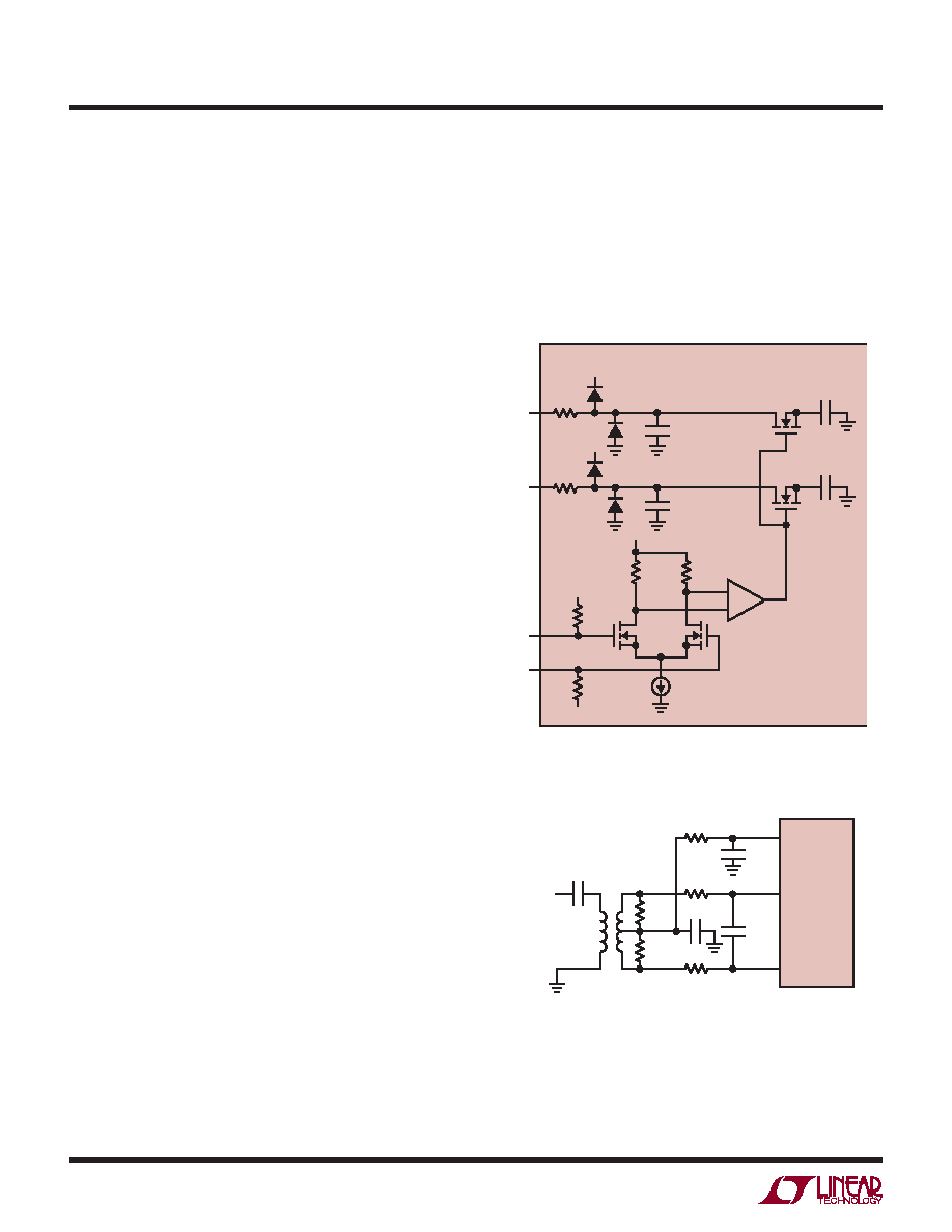
ANALOG INPUT
The analog inputs are differential CMOS sample-and-hold
circuits(Figure2).Theinputsshouldbedrivendifferentially
around a common mode voltage set by the VCM1 or VCM2
output pins, which are nominally VDD/2. For the 2V input
range, the inputs should swing from VCM – 0.5V to VCM
+ 0.5V. There should be a 180° phase difference between
the inputs.
The two channels are simultaneously sampled by a
shared encode circuit (Figure 2).
INPUT DRIVE CIRCUITS
Input Filtering
If possible, there should be an RC lowpass filter right
at the analog inputs. This lowpass filter isolates the
drive circuitry from the A/D sample-and-hold switching
and limits wideband noise from the drive circuitry.
Figure 3 shows an example of an input RC filter. The
RC component values should be chosen based on the
application’s input frequency.
APPLICATIONS INFORMATION
Transformer Coupled Circuits
Figure 3 shows the analog input being driven by an RF
transformer with a center-tapped secondary. The center
tap is biased with VCM, setting the A/D input at its opti-
mal DC level. At higher input frequencies a transmission
line balun transformer (Figures 4 to 6) has better balance,
resulting in lower A/D distortion.
CSAMPLE
3.5pF
RON
25
RON
25
VDD
LTC2265-12
AIN+
226512 F02
CSAMPLE
3.5pF
VDD
AIN–
ENC–
ENC+
1.2V
10k
1.2V
10k
CPARASITIC
1.8pF
CPARASITIC
1.8pF
10
Figure 2. Equivalent Input Circuit. Only One of
the Two Analog Channels Is Shown.
25
50
0.1F
AIN+
AIN–
12pF
0.1F
VCM
LTC2265-12
ANALOG
INPUT
0.1F
T1
1:1
T1: MA/COM MABAES0060
RESISTORS, CAPACITORS
ARE 0402 PACKAGE SIZE
226512 F03
Figure 3. Analog Input Circuit Using a Transformer.
Recommended for Input Frequencies from 5MHz to 70MHz
相关PDF资料 |
PDF描述 |
|---|---|
| LTC2268IUJ-14#TRPBF | IC ADC 14BIT 125MSPS DUAL 40QFN |
| LTC2280CUP#PBF | IC ADC DUAL 10BIT 105MSPS 64-QFN |
| LTC2281IUP#PBF | IC ADC 10BIT DUAL 64-QFN |
| LTC2282CUP#PBF | IC ADC DUAL 12BIT 105MSPS 64-QFN |
| LTC2284CUP#PBF | IC ADC DUAL 14BIT 105MSPS 64-QFN |
相关代理商/技术参数 |
参数描述 |
|---|---|
| LTC2264CUJ-12TRPBF | 制造商:LINER 制造商全称:Linear Technology 功能描述:12-Bit, 65Msps/40Msps/25Msps Low Power Dual ADCs |
| LTC2264CUJ-14 | 制造商:LINER 制造商全称:Linear Technology 功能描述:14-Bit, 65Msps/40Msps/25Msps Low Power Dual ADCs |
| LTC2264CUJ-14#PBF | 功能描述:IC ADC 14BIT SER/PAR 40M 40-QFN RoHS:是 类别:集成电路 (IC) >> 数据采集 - 模数转换器 系列:- 其它有关文件:TSA1204 View All Specifications 标准包装:1 系列:- 位数:12 采样率(每秒):20M 数据接口:并联 转换器数目:2 功率耗散(最大):155mW 电压电源:模拟和数字 工作温度:-40°C ~ 85°C 安装类型:表面贴装 封装/外壳:48-TQFP 供应商设备封装:48-TQFP(7x7) 包装:Digi-Reel® 输入数目和类型:4 个单端,单极;2 个差分,单极 产品目录页面:1156 (CN2011-ZH PDF) 其它名称:497-5435-6 |
| LTC2264CUJ-14#TRPBF | 功能描述:IC ADC 14BIT SER/PAR 40M 40-QFN RoHS:是 类别:集成电路 (IC) >> 数据采集 - 模数转换器 系列:- 标准包装:1 系列:- 位数:14 采样率(每秒):83k 数据接口:串行,并联 转换器数目:1 功率耗散(最大):95mW 电压电源:双 ± 工作温度:0°C ~ 70°C 安装类型:通孔 封装/外壳:28-DIP(0.600",15.24mm) 供应商设备封装:28-PDIP 包装:管件 输入数目和类型:1 个单端,双极 |
| LTC2264CUJ-14PBF | 制造商:LINER 制造商全称:Linear Technology 功能描述:14-Bit, 65Msps/40Msps/25Msps Low Power Dual ADCs |
发布紧急采购,3分钟左右您将得到回复。