- 您现在的位置:买卖IC网 > PDF目录39416 > LTC2265IUJ-12#PBF (LINEAR TECHNOLOGY CORP) PROPRIETARY METHOD ADC, QCC40 PDF资料下载
参数资料
| 型号: | LTC2265IUJ-12#PBF |
| 厂商: | LINEAR TECHNOLOGY CORP |
| 元件分类: | ADC |
| 英文描述: | PROPRIETARY METHOD ADC, QCC40 |
| 封装: | 6 X 6 MM, LEAD FREE, PLASTIC, QFN-40 |
| 文件页数: | 32/34页 |
| 文件大小: | 1231K |
| 代理商: | LTC2265IUJ-12#PBF |
第1页第2页第3页第4页第5页第6页第7页第8页第9页第10页第11页第12页第13页第14页第15页第16页第17页第18页第19页第20页第21页第22页第23页第24页第25页第26页第27页第28页第29页第30页第31页当前第32页第33页第34页
LTC2265-12/
LTC2264-12/LTC2263-12
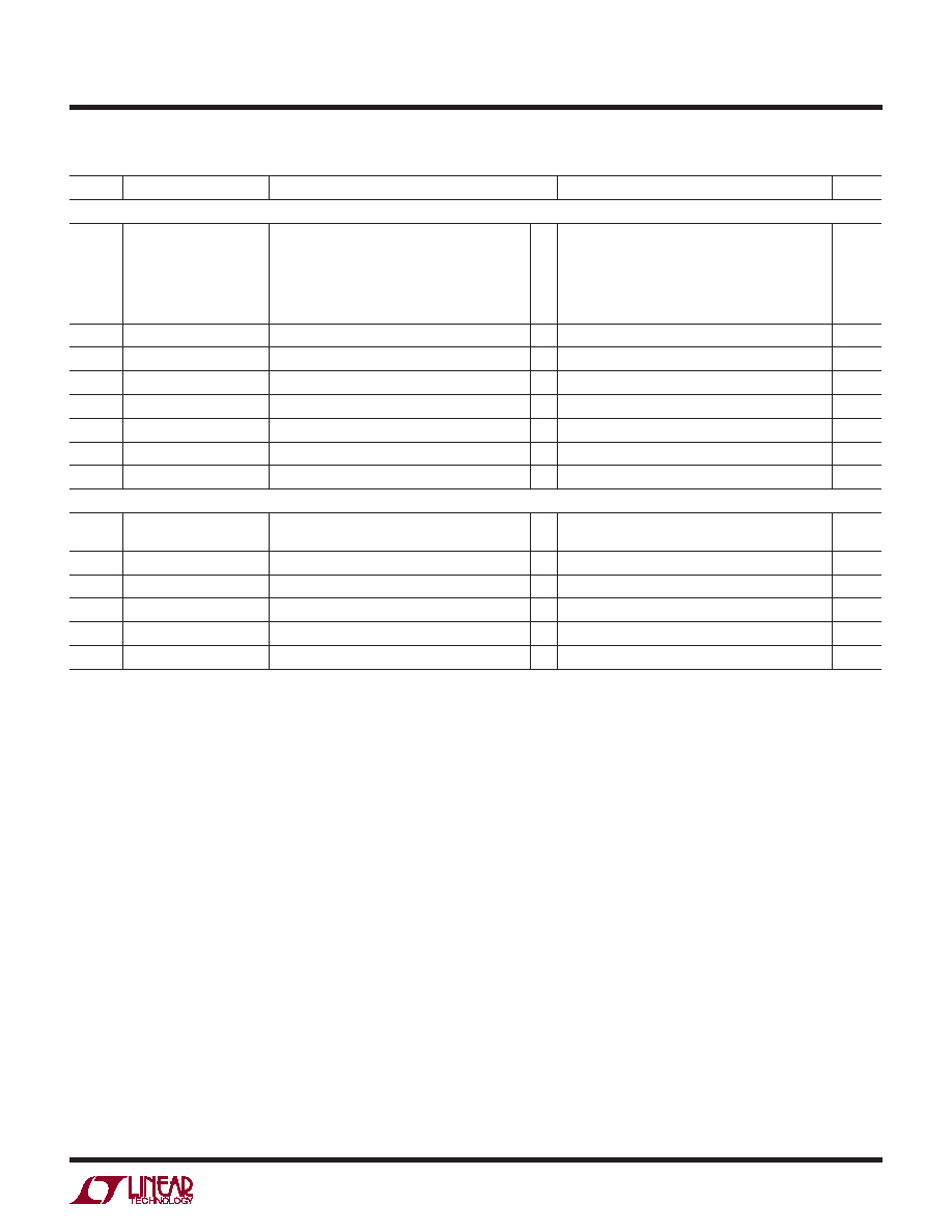
7
22654312fb
TIMING CHARACTERISTICS The
l
denotes the specifications which apply over the full operating temperature
range, otherwise specifications are at TA = 25°C. (Note 5)
SYMBOL PARAMETER
CONDITIONS
MIN
TYP
MAX
UNITS
Digital Data Outputs (RTERM = 100Ω Differential, CL = 2pF to GND on Each Output)
tSER
Serial Data Bit Period
Two Lanes, 16-Bit Serialization
Two Lanes, 14-Bit Serialization
Two Lanes, 12-Bit Serialization
One Lane, 16-Bit Serialization
One Lane, 14-Bit Serialization
One Lane, 12-Bit Serialization
1 / (8 fS)
1 / (7 fS)
1 / (6 fS)
1 / (16 fS)
1 / (14 fS)
1 / (12 fS)
s
tFRAME
FR to DCO Delay
(Note 8)
l
0.35 tSER
0.5 tSER
0.65 tSER
s
tDATA
DATA to DCO Delay
(Note 8)
l
0.35 tSER
0.5 tSER
0.65 tSER
s
tPD
Propagation Delay
(Note 8)
l
0.7n + 2 tSER 1.1n + 2 tSER 1.5n + 2 tSER
s
tR
Output Rise Time
Data, DCO, FR, 20% to 80%
0.17
ns
tF
Output Fall Time
Data, DCO, FR, FR, 20% to 80%
0.17
ns
DCO Cycle-to-Cycle Jitter tSER = 1ns
60
psP-P
Pipeline Latency
6
Cycles
SPI Port Timing (Note 8)
tSCK
SCK Period
Write Mode
Readback Mode, CSDO = 20pF, RPULLUP = 2k
l
40
250
ns
tS
CS to SCK Set-Up Time
l
5
ns
tH
SCK to CS Set-Up Time
l
5
ns
tDS
SDI Set-Up Time
l
5
ns
tDH
SDI Hold Time
l
5
ns
tDO
SCK Falling to SDO Valid
Readback Mode, CSDO = 20pF, RPULLUP = 2k
l
125
ns
Note 1: Stresses beyond those listed under Absolute Maximum Ratings
may cause permanent damage to the device. Exposure to any Absolute
Maximum Rating condition for extended periods may affect device
reliability and lifetime.
Note 2: All voltage values are with respect to GND with GND and OGND
shorted (unless otherwise noted).
Note 3: When these pin voltages are taken below GND or above VDD, they
will be clamped by internal diodes. This product can handle input currents
of greater than 100mA below GND or above VDD without latchup.
Note 4: When these pin voltages are taken below GND they will be
clamped by internal diodes. When these pin voltages are taken above VDD
they will not be clamped by internal diodes. This product can handle input
currents of greater than 100mA below GND without latchup.
Note 5: VDD = OVDD = 1.8V, fSAMPLE = 65MHz (LTC2265), 40MHz
(LTC2264), or 25MHz (LTC2263), 2-lane output mode, differential ENC+/
ENC– = 2VP-P sine wave, input range = 2VP-P with differential drive, unless
otherwise noted.
Note 6: Integral nonlinearity is defined as the deviation of a code from a
best fit straight line to the transfer curve. The deviation is measured from
the center of the quantization band.
Note 7: Offset error is the offset voltage measured from –0.5 LSB when
the output code flickers between 0000 0000 0000 and 1111 1111 1111 in
2’s complement output mode.
Note 8: Guaranteed by design, not subject to test.
Note 9: VDD = OVDD = 1.8V, fSAMPLE = 65MHz (LTC2265), 40MHz
(LTC2264), or 25MHz (LTC2263), 2-lane output mode, ENC+ = single-
ended 1.8V square wave, ENC– = 0V, input range = 2VP-P with differential
drive, unless otherwise noted. The supply current and power dissipation
specifications are totals for the entire chip, not per channel.
Note 10: Recommended operating conditions.
Note 11: The maximum sampling frequency depends on the speed grade
of the part and also which serialization mode is used. The maximum serial
data rate is 1000Mbps, so tSER must be greater than or equal to 1ns.
相关PDF资料 |
PDF描述 |
|---|---|
| LTC2265CUJ-12#TRPBF | PROPRIETARY METHOD ADC, QCC40 |
| LTC2263CUJ-12#PBF | PROPRIETARY METHOD ADC, QCC40 |
| LTC2264CUJ-12#TRPBF | PROPRIETARY METHOD ADC, QCC40 |
| LTC2263CUJ-12#TRPBF | PROPRIETARY METHOD ADC, QCC40 |
| LTC2264IUJ-12#PBF | PROPRIETARY METHOD ADC, QCC40 |
相关代理商/技术参数 |
参数描述 |
|---|---|
| LTC2265IUJ-12TRPBF | 制造商:LINER 制造商全称:Linear Technology 功能描述:12-Bit, 65Msps/40Msps/25Msps Low Power Dual ADCs |
| LTC2265IUJ-14 | 制造商:LINER 制造商全称:Linear Technology 功能描述:14-Bit, 65Msps/40Msps/25Msps Low Power Dual ADCs |
| LTC2265IUJ-14#PBF | 功能描述:IC ADC 14BIT SER/PAR 65M 40-QFN RoHS:是 类别:集成电路 (IC) >> 数据采集 - 模数转换器 系列:- 其它有关文件:TSA1204 View All Specifications 标准包装:1 系列:- 位数:12 采样率(每秒):20M 数据接口:并联 转换器数目:2 功率耗散(最大):155mW 电压电源:模拟和数字 工作温度:-40°C ~ 85°C 安装类型:表面贴装 封装/外壳:48-TQFP 供应商设备封装:48-TQFP(7x7) 包装:Digi-Reel® 输入数目和类型:4 个单端,单极;2 个差分,单极 产品目录页面:1156 (CN2011-ZH PDF) 其它名称:497-5435-6 |
| LTC2265IUJ-14#TRPBF | 功能描述:IC ADC 14BIT SER/PAR 65M 40-QFN RoHS:是 类别:集成电路 (IC) >> 数据采集 - 模数转换器 系列:- 标准包装:1 系列:- 位数:14 采样率(每秒):83k 数据接口:串行,并联 转换器数目:1 功率耗散(最大):95mW 电压电源:双 ± 工作温度:0°C ~ 70°C 安装类型:通孔 封装/外壳:28-DIP(0.600",15.24mm) 供应商设备封装:28-PDIP 包装:管件 输入数目和类型:1 个单端,双极 |
| LTC2265IUJ-14PBF | 制造商:LINER 制造商全称:Linear Technology 功能描述:14-Bit, 65Msps/40Msps/25Msps Low Power Dual ADCs |
发布紧急采购,3分钟左右您将得到回复。