- 您现在的位置:买卖IC网 > PDF目录224114 > LTC2281IUP (LINEAR TECHNOLOGY CORP) Dual 10-Bit, 125Msps Low Power 3V ADC; Package: QFN; No of Pins: 64; Temperature Range: -40°C to +85°C PDF资料下载
参数资料
| 型号: | LTC2281IUP |
| 厂商: | LINEAR TECHNOLOGY CORP |
| 元件分类: | ADC |
| 英文描述: | Dual 10-Bit, 125Msps Low Power 3V ADC; Package: QFN; No of Pins: 64; Temperature Range: -40°C to +85°C |
| 中文描述: | DUAL 1-CH 10-BIT PROPRIETARY METHOD ADC, PARALLEL ACCESS, PQCC64 |
| 封装: | 9 X 9 MM, PLASTIC, MO-220WNJR-5, QFN-64 |
| 文件页数: | 1/24页 |
| 文件大小: | 500K |
| 代理商: | LTC2281IUP |
LTC2281
1
2281fb
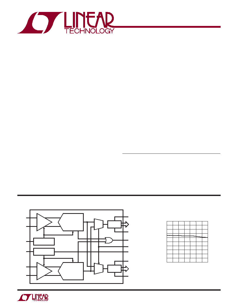
TYPICAL APPLICATION
FEATURES
APPLICATIONS
DESCRIPTION
Dual 10-Bit, 125Msps
Low Power 3V ADC
The LTC2281 is a 10-bit 125Msps, low power dual 3V
A/D converter designed for digitizing high frequency,
wide dynamic range signals. The LTC2281 is perfect for
demanding imaging and communications applications
with AC performance that includes 61.6dB SNR and 82dB
SFDR for signals at the Nyquist frequency.
Typical DC specs include ±0.1LSB INL, ±0.1LSB DNL. The
transition noise is a low 0.08LSBRMS.
A single 3V supply allows low power operation. A separate
output supply allows the outputs to drive 0.5V to 3.6V
logic.
A single-ended CLK input controls converter operation.
An optional clock duty cycle stabilizer allows high perfor-
mance at full speed for a wide range of clock duty cycles.
A data ready output clock (CLKOUT) can be used to latch
the output data.
SNR vs Input Frequency,
–1dB, 2V Range
n Integrated Dual 10-Bit ADCs
n Sample Rate: 125Msps
n Single 3V Supply (2.85V to 3.4V)
n Low Power: 790mW
n 61.6dB SNR, 88dB SFDR
n 110dB Channel Isolation at 100MHz
n Flexible Input: 1VP-P to 2VP-P Range
n 640MHz Full Power Bandwidth S/H
n Clock Duty Cycle Stabilizer
n Shutdown and Nap Modes
n Data Ready Output Clock
n Pin Compatible Family
125Msps: LTC2283 (12-Bit), LTC2281 (10-Bit)
105Msps: LTC2282 (12-Bit), LTC2280 (10-Bit)
80Msps: LTC2294 (12-Bit), LTC2289 (10-Bit)
65Msps: LTC2293 (12-Bit), LTC2288 (10-Bit)
40Msps: LTC2292 (12-Bit), LTC2287 (10-Bit)
n 64-Pin (9mm × 9mm) QFN Package
n Wireless and Wired Broadband Communication
n Imaging Systems
n Spectral Analysis
n Portable Instrumentation
L, LT, LTC and LTM are registered trademarks of Linear Technology Corporation. All other
trademarks are the property of their respective owners.
–
+
INPUT
S/H
ANALOG
INPUT A
ANALOG
INPUT B
CLK A
CLK B
10-BIT
PIPELINED
ADC CORE
CLOCK/DUTY CYCLE
CONTROL
OUTPUT
DRIVERS
OVDD
OGND
MUX
CLKOUT
D9A
D0A
OVDD
OGND
2281 TA01
D9B
D0B
–
+
OUTPUT
DRIVERS
INPUT
S/H
10-BIT
PIPELINED
ADC CORE
CLOCK/DUTY CYCLE
CONTROL
OF
INPUT FREQUENCY (MHz)
0
55
SNR
(dBFS)
56
58
59
60
65
62
100
200
250
2281 TA01b
57
63
64
61
50
150
300
350
相关PDF资料 |
PDF描述 |
|---|---|
| LTC2281IUP#TR | Dual 10-Bit, 125Msps Low Power 3V ADC; Package: QFN; No of Pins: 64; Temperature Range: -40°C to +85°C |
| LTC2282CUP | Dual 12-Bit, 105Msps Low Power 3V ADC; Package: QFN; No of Pins: 64; Temperature Range: 0°C to +70°C |
| LTC2282CUP#TR | Dual 12-Bit, 105Msps Low Power 3V ADC; Package: QFN; No of Pins: 64; Temperature Range: 0°C to +70°C |
| LTC2282IUP | Dual 12-Bit, 105Msps Low Power 3V ADC; Package: QFN; No of Pins: 64; Temperature Range: -40°C to +85°C |
| LTC2282IUP#TR | Dual 12-Bit, 105Msps Low Power 3V ADC; Package: QFN; No of Pins: 64; Temperature Range: -40°C to +85°C |
相关代理商/技术参数 |
参数描述 |
|---|---|
| LTC2281IUP#PBF | 功能描述:IC ADC 10BIT DUAL 64-QFN RoHS:是 类别:集成电路 (IC) >> 数据采集 - 模数转换器 系列:- 标准包装:1 系列:- 位数:14 采样率(每秒):83k 数据接口:串行,并联 转换器数目:1 功率耗散(最大):95mW 电压电源:双 ± 工作温度:0°C ~ 70°C 安装类型:通孔 封装/外壳:28-DIP(0.600",15.24mm) 供应商设备封装:28-PDIP 包装:管件 输入数目和类型:1 个单端,双极 |
| LTC2281IUP#TRPBF | 功能描述:IC ADC DUAL 10BIT 125MSPS 64QFN RoHS:是 类别:集成电路 (IC) >> 数据采集 - 模数转换器 系列:- 标准包装:1 系列:- 位数:14 采样率(每秒):83k 数据接口:串行,并联 转换器数目:1 功率耗散(最大):95mW 电压电源:双 ± 工作温度:0°C ~ 70°C 安装类型:通孔 封装/外壳:28-DIP(0.600",15.24mm) 供应商设备封装:28-PDIP 包装:管件 输入数目和类型:1 个单端,双极 |
| LTC2281IUP-PBF | 制造商:LINER 制造商全称:Linear Technology 功能描述:Dual 10-Bit, 125Msps Low Power 3V ADC |
| LTC2281IUP-TR | 制造商:LINER 制造商全称:Linear Technology 功能描述:Dual 10-Bit, 125Msps Low Power 3V ADC |
| LTC2281IUP-TRPBF | 制造商:LINER 制造商全称:Linear Technology 功能描述:Dual 10-Bit, 125Msps Low Power 3V ADC |
发布紧急采购,3分钟左右您将得到回复。