- 您现在的位置:买卖IC网 > PDF目录2005 > LTC2284CUP#PBF (Linear Technology)IC ADC DUAL 14BIT 105MSPS 64-QFN PDF资料下载
参数资料
| 型号: | LTC2284CUP#PBF |
| 厂商: | Linear Technology |
| 文件页数: | 7/24页 |
| 文件大小: | 0K |
| 描述: | IC ADC DUAL 14BIT 105MSPS 64-QFN |
| 标准包装: | 40 |
| 位数: | 14 |
| 采样率(每秒): | 105M |
| 数据接口: | 并联 |
| 转换器数目: | 2 |
| 功率耗散(最大): | 630mW |
| 电压电源: | 单电源 |
| 工作温度: | 0°C ~ 70°C |
| 安装类型: | 表面贴装 |
| 封装/外壳: | 64-WFQFN 裸露焊盘 |
| 供应商设备封装: | 64-QFN(9x9) |
| 包装: | 管件 |
| 输入数目和类型: | 2 个单端,双极; 2 个差分, 双极 |
LTC2284
15
2284fa
VCM
SENSE
1.5V
0.75V
2.2
F
12k
1
F
12k
2284 F10
LTC2284
VCM
REFH
SENSE
TIE TO VDD FOR 2V RANGE;
TIE TO VCM FOR 1V RANGE;
RANGE = 2 VSENSE FOR
0.5V < VSENSE < 1V
1.5V
REFL
2.2
F
2.2
F
INTERNAL ADC
HIGH REFERENCE
BUFFER
0.1
F
2284 F09
4
DIFF AMP
1
F
1
F
INTERNAL ADC
LOW REFERENCE
1.5V BANDGAP
REFERENCE
1V
0.5V
RANGE
DETECT
AND
CONTROL
LTC2284
APPLICATIO S I FOR ATIO
WU
UU
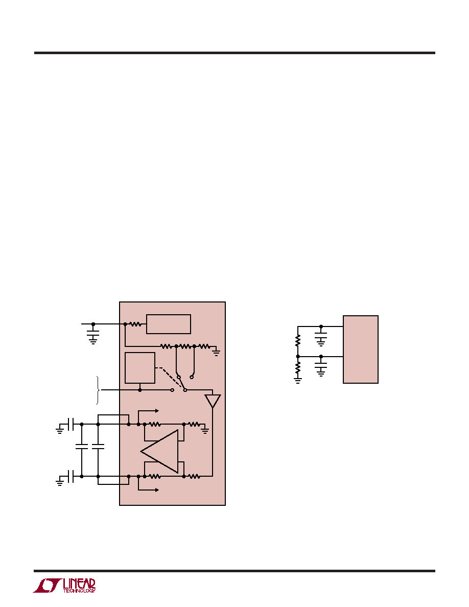
Reference Operation
Figure 9 shows the LTC2284 reference circuitry consisting
of a 1.5V bandgap reference, a difference amplifier and
switching and control circuit. The internal voltage refer-
ence can be configured for two pin selectable input ranges
of 2V (
±1Vdifferential)or1V(±0.5Vdifferential).Tyingthe
SENSE pin to VDD selects the 2V range; tying the SENSE
pin to VCM selects the 1V range.
The 1.5V bandgap reference serves two functions: its
output provides a DC bias point for setting the common
mode voltage of any external input circuitry; additionally,
the reference is used with a difference amplifier to gener-
ate the differential reference levels needed by the internal
ADC circuitry. An external bypass capacitor is required for
the 1.5V reference output, VCM. This provides a high
frequency low impedance path to ground for internal and
external circuitry.
The difference amplifier generates the high and low refer-
ence for the ADC. High speed switching circuits are
connected to these outputs and they must be externally
bypassed. Each output has two pins. The multiple output
pins are needed to reduce package inductance. Bypass
capacitors must be connected as shown in Figure 9. Each
ADC channel has an independent reference with its own
bypass capacitors. The two channels can be used with the
same or different input ranges.
Other voltage ranges between the pin selectable ranges
can be programmed with two external resistors as shown
in Figure 10. An external reference can be used by applying
its output directly or through a resistor divider to SENSE.
It is not recommended to drive the SENSE pin with a logic
device. The SENSE pin should be tied to the appropriate
level as close to the converter as possible. If the SENSE pin
is driven externally, it should be bypassed to ground as
close to the device as possible with a 1
F ceramic capacitor.
For the best channel matching, connect an external reference
to SENSEA and SENSEB.
Figure 10. 1.5V Range ADC
Figure 9. Equivalent Reference Circuit
Input Range
The input range can be set based on the application. The
2V input range will provide the best signal-to-noise perfor-
mance while maintaining excellent SFDR. The 1V input
range will have better SFDR performance, but the SNR will
degrade by 5.7dB. See the Typical Performance Charac-
teristics section.
Driving the Clock Input
The CLK inputs can be driven directly with a CMOS or TTL
level signal. A sinusoidal clock can also be used along with
a low jitter squaring circuit before the CLK pin (Figure 11).
相关PDF资料 |
PDF描述 |
|---|---|
| LTC2285CUP#PBF | IC ADC DUAL 14BIT 125MSPS 64QFN |
| LTC2289IUP#PBF | IC ADC DUAL 10BIT 80MSPS 64QFN |
| LTC2290IUP#TRPBF | IC ADC DUAL 12BIT 10MSPS 64QFN |
| LTC2298IUP#PBF | IC ADC DUAL 14BIT 65MSPS 64QFN |
| LTC2305CDE#TRPBF | IC ADC 12-BIT 2CHN 12-DFN |
相关代理商/技术参数 |
参数描述 |
|---|---|
| LTC2284IUP | 制造商:Linear Technology 功能描述:ADC Dual Pipelined 105Msps 14-bit Parallel 64-Pin QFN EP |
| LTC2284IUP#PBF | 功能描述:IC ADC DUAL 14BIT 105MSPS 64-QFN RoHS:是 类别:集成电路 (IC) >> 数据采集 - 模数转换器 系列:- 标准包装:1 系列:microPOWER™ 位数:8 采样率(每秒):1M 数据接口:串行,SPI? 转换器数目:1 功率耗散(最大):- 电压电源:模拟和数字 工作温度:-40°C ~ 125°C 安装类型:表面贴装 封装/外壳:24-VFQFN 裸露焊盘 供应商设备封装:24-VQFN 裸露焊盘(4x4) 包装:Digi-Reel® 输入数目和类型:8 个单端,单极 产品目录页面:892 (CN2011-ZH PDF) 其它名称:296-25851-6 |
| LTC2284IUP#PBF | 制造商:Linear Technology 功能描述:A/D Converter (A-D) IC 制造商:Linear Technology 功能描述:IC, ADC, 14BIT, 105MSPS, QFN-64 |
| LTC2284IUP#TRPBF | 功能描述:IC ADC DUAL 14BIT 105MSPS 64-QFN RoHS:是 类别:集成电路 (IC) >> 数据采集 - 模数转换器 系列:- 产品培训模块:Lead (SnPb) Finish for COTS Obsolescence Mitigation Program 标准包装:250 系列:- 位数:12 采样率(每秒):1.8M 数据接口:并联 转换器数目:1 功率耗散(最大):1.82W 电压电源:模拟和数字 工作温度:-40°C ~ 85°C 安装类型:表面贴装 封装/外壳:48-LQFP 供应商设备封装:48-LQFP(7x7) 包装:管件 输入数目和类型:2 个单端,单极 |
| LTC2284UP | 制造商:LINER 制造商全称:Linear Technology 功能描述:Dual 14-Bit, 105Msps Low Power 3V ADC |
发布紧急采购,3分钟左右您将得到回复。