- 您现在的位置:买卖IC网 > PDF目录10036 > LTC2285CUP#TRPBF (Linear Technology)IC ADC DUAL 14BIT 125MSPS 64QFN PDF资料下载
参数资料
| 型号: | LTC2285CUP#TRPBF |
| 厂商: | Linear Technology |
| 文件页数: | 9/24页 |
| 文件大小: | 0K |
| 描述: | IC ADC DUAL 14BIT 125MSPS 64QFN |
| 标准包装: | 2,000 |
| 位数: | 14 |
| 采样率(每秒): | 125M |
| 数据接口: | 并联 |
| 转换器数目: | 2 |
| 功率耗散(最大): | 915mW |
| 电压电源: | 单电源 |
| 工作温度: | 0°C ~ 70°C |
| 安装类型: | 表面贴装 |
| 封装/外壳: | 64-WFQFN 裸露焊盘 |
| 供应商设备封装: | 64-QFN(9x9) |
| 包装: | 带卷 (TR) |
| 输入数目和类型: | 2 个单端,双极; 2 个差分, 双极 |
LTC2285
17
2285fb
APPLICATIONS INFORMATION
small valued capacitors. Junction leakage will discharge
the capacitors. The specied minimum operating frequency
for the LTC2285 is 1Msps.
Clock Duty Cycle Stabilizer
An optional clock duty cycle stabilizer circuit ensures
high performance even if the input clock has a non
50% duty cycle. Using the clock duty cycle stabilizer is
recommended for most applications. To use the clock
duty cycle stabilizer, the MODE pin should be connected
to 1/3VDD or 2/3VDD using external resistors.
This circuit uses the rising edge of the CLK pin to sample
the analog input. The falling edge of CLK is ignored and
the internal falling edge is generated by a phase-locked
loop. The input clock duty cycle can vary from 40% to 60%
and the clock duty cycle stabilizer will maintain a constant
50% internal duty cycle. If the clock is turned off for a
long period of time, the duty cycle stabilizer circuit will
require a hundred clock cycles for the PLL to lock onto the
input clock.
For applications where the sample rate needs to be changed
quickly, the clock duty cycle stabilizer can be disabled. If
the duty cycle stabilizer is disabled, care should be taken to
make the sampling clock have a 50% (±5%) duty cycle.
DIGITAL OUTPUTS
Table 1 shows the relationship between the analog input
voltage, the digital data bits, and the overow bit. Note that
OF is high when an overow or underow has occurred
on either channel A or channel B.
Table 1. Output Codes vs Input Voltage
AIN+ – AIN–
(2V Range)
OF
D13 – D0
(Offset Binary)
D13 – D0
(2’s Complement)
>+1.000000V
+0.999878V
+0.999756V
1
0
11 1111 1111 1111
11 1111 1111 1110
01 1111 1111 1111
01 1111 1111 1110
+0.000122V
0.000000V
–0.000122V
–0.000244V
0
10 0000 0000 0001
10 0000 0000 0000
01 1111 1111 1111
01 1111 1111 1110
00 0000 0000 0001
00 0000 0000 0000
11 1111 1111 1111
11 1111 1111 1110
–0.999878V
–1.000000V
<–1.000000V
0
1
00 0000 0000 0001
00 0000 0000 0000
10 0000 0000 0001
10 0000 0000 0000
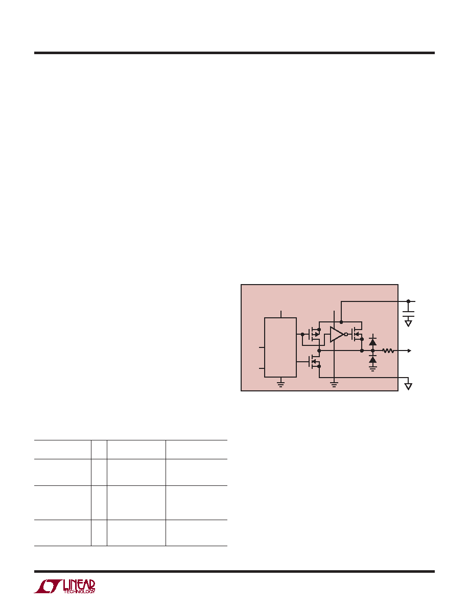
Digital Output Buffers
Figure 14 shows an equivalent circuit for a single out-
put buffer. Each buffer is powered by OVDD and OGND,
isolated from the ADC power and ground. The additional
N-channel transistor in the output driver allows operation
down to low voltages. The internal resistor in series with
the output makes the output appear as 50Ω to external
circuitry and may eliminate the need for external damping
resistors.
As with all high speed/high resolution converters, the
digital output loading can affect the performance. The
digital outputs of the LTC2285 should drive a minimal
capacitive load to avoid possible interaction between the
digital outputs and sensitive input circuitry. For full speed
operation the capacitive load should be kept under 10pF.
Lower OVDD voltages will also help reduce interference
from the digital outputs.
Figure 14. Digital Output Buffer
LTC2283
2283 F14
OVDD
VDD
0.1μF
43Ω
TYPICAL
DATA
OUTPUT
OGND
OVDD
0.5V
TO 3.6V
PREDRIVER
LOGIC
DATA
FROM
LATCH
OE
Data Format
Using the MODE pin, the LTC2285 parallel digital output
can be selected for offset binary or 2’s complement format.
Connecting MODE to GND or 1/3VDD selects offset binary
output format. Connecting MODE to 2/3VDD or VDD selects
2’s complement output format. An external resistor divider
can be used to set the 1/3VDD or 2/3VDD logic values.
Table 2 shows the logic states for the MODE pin.
相关PDF资料 |
PDF描述 |
|---|---|
| LTC486ISW | IC DVR RS485 LOW PWR QUAD 16SOIC |
| IDT72V3611L20PF8 | IC FIFO SYNC 64X36 20NS 120-TQFP |
| MS27656E17A35SD | CONN RCPT 55POS WALL MNT W/SCKT |
| MS27497T10B99S | CONN RCPT 7POS WALL MNT W/SCKT |
| IDT7285L15PAI8 | IC FIFO 4096X18 15NS 56TSSOP |
相关代理商/技术参数 |
参数描述 |
|---|---|
| LTC2285IUP | 制造商:Linear Technology 功能描述:ADC Dual Pipelined 125Msps 14-bit Parallel 64-Pin QFN EP |
| LTC2285IUP#PBF | 功能描述:IC ADC DUAL 14BIT 125MSPS 64QFN RoHS:是 类别:集成电路 (IC) >> 数据采集 - 模数转换器 系列:- 标准包装:1 系列:microPOWER™ 位数:8 采样率(每秒):1M 数据接口:串行,SPI? 转换器数目:1 功率耗散(最大):- 电压电源:模拟和数字 工作温度:-40°C ~ 125°C 安装类型:表面贴装 封装/外壳:24-VFQFN 裸露焊盘 供应商设备封装:24-VQFN 裸露焊盘(4x4) 包装:Digi-Reel® 输入数目和类型:8 个单端,单极 产品目录页面:892 (CN2011-ZH PDF) 其它名称:296-25851-6 |
| LTC2285IUP#TRPBF | 功能描述:IC ADC DUAL 14BIT 125MSPS 64QFN RoHS:是 类别:集成电路 (IC) >> 数据采集 - 模数转换器 系列:- 产品培训模块:Lead (SnPb) Finish for COTS Obsolescence Mitigation Program 标准包装:250 系列:- 位数:12 采样率(每秒):1.8M 数据接口:并联 转换器数目:1 功率耗散(最大):1.82W 电压电源:模拟和数字 工作温度:-40°C ~ 85°C 安装类型:表面贴装 封装/外壳:48-LQFP 供应商设备封装:48-LQFP(7x7) 包装:管件 输入数目和类型:2 个单端,单极 |
| LTC2285IUP-3CGPBF | 制造商:LINER 制造商全称:Linear Technology 功能描述:Dual 14-Bit, 135Msps Low Power 3.3V ADC |
| LTC2285IUPPBF | 制造商:Linear Technology 功能描述:ADC, Dual 14b 125Msps, 3V, LTC2285IUP |
发布紧急采购,3分钟左右您将得到回复。