- 您现在的位置:买卖IC网 > PDF目录10664 > LTC2290CUP#PBF (Linear Technology)IC ADC DUAL 12BIT 10MSPS 64QFN PDF资料下载
参数资料
| 型号: | LTC2290CUP#PBF |
| 厂商: | Linear Technology |
| 文件页数: | 20/24页 |
| 文件大小: | 0K |
| 描述: | IC ADC DUAL 12BIT 10MSPS 64QFN |
| 标准包装: | 40 |
| 位数: | 12 |
| 采样率(每秒): | 10M |
| 数据接口: | 并联 |
| 转换器数目: | 2 |
| 功率耗散(最大): | 138mW |
| 电压电源: | 单电源 |
| 工作温度: | 0°C ~ 70°C |
| 安装类型: | 表面贴装 |
| 封装/外壳: | 64-WFQFN 裸露焊盘 |
| 供应商设备封装: | 64-QFN(9x9) |
| 包装: | 管件 |
| 输入数目和类型: | 2 个单端,双极; 2 个差分, 双极 |
| 产品目录页面: | 1349 (CN2011-ZH PDF) |
LTC2290
5
2290fa
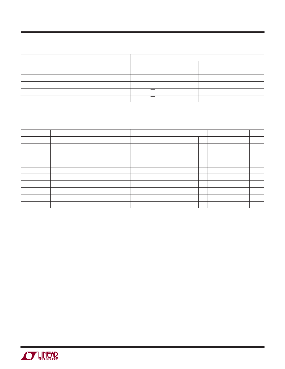
SYMBOL
PARAMETER
CONDITIONS
MIN
TYP
MAX
UNITS
fs
Sampling Frequency
(Note 9)
●
1
10
MHz
tL
CLK Low Time
Duty Cycle Stabilizer Off
●
40
50
500
ns
Duty Cycle Stabilizer On (Note 7)
●
5
50
500
ns
tH
CLK High Time
Duty Cycle Stabilizer Off
●
40
50
500
ns
Duty Cycle Stabilizer On (Note 7)
●
5
50
500
ns
tAP
Sample-and-Hold Aperture Delay
0
nS
tD
CLK to DATA Delay
CL = 5pF (Note 7)
●
1.4
2.7
5.4
ns
tMD
MUX to DATA Delay
CL = 5pF (Note 7)
●
1.4
2.7
5.4
ns
Data Access Time After OE
↓
CL = 5pF (Note 7)
●
4.3
10
ns
BUS Relinquish Time
(Note 7)
●
3.3
8.5
ns
Pipeline Latency
5
Cycles
POWER REQUIRE E TS
W
U
The
● denotes the specifications which apply over the full operating temperature
range, otherwise specifications are at TA = 25°C. (Note 8)
TI I G CHARACTERISTICS
U
W
The
● denotes the specifications which apply over the full operating temperature
range, otherwise specifications are at TA = 25°C. (Note 4)
Note 1: Stresses beyond those listed under Absolute Maximum Ratings
may cause permanent damage to the device. Exposure to any Absolute
Maximum Rating condition for extended periods may affect device
reliability and lifetime.
Note 2: All voltage values are with respect to ground with GND and OGND
wired together (unless otherwise noted).
Note 3: When these pin voltages are taken below GND or above VDD, they
will be clamped by internal diodes. This product can handle input currents
of greater than 100mA below GND or above VDD without latchup.
Note 4: VDD = 3V, fSAMPLE = 10MHz, input range = 2VP-P with differential
drive, unless otherwise noted.
Note 5: Integral nonlinearity is defined as the deviation of a code from a
straight line passing through the actual endpoints of the transfer curve.
The deviation is measured from the center of the quantization band.
Note 6: Offset error is the offset voltage measured from –0.5 LSB when
the output code flickers between 0000 0000 0000 and 1111 1111 1111.
Note 7: Guaranteed by design, not subject to test.
Note 8: VDD = 3V, fSAMPLE = 10MHz, input range = 1VP-P with differential
drive. The supply current and power dissipation are the sum total for both
channels with both channels active.
Note 9: Recommended operating conditions.
SYMBOL
PARAMETER
CONDITIONS
MIN
TYP
MAX
UNITS
VDD
Analog Supply Voltage
(Note 9)
●
2.7
3
3.4
V
OVDD
Output Supply Voltage
(Note 9)
●
0.5
3
3.6
V
IVDD
Supply Current
Both ADCs at fS(MAX)
●
40
46
mA
PDISS
Power Dissipation
Both ADCs at fS(MAX)
●
120
138
mW
PSHDN
Shutdown Power (Each Channel)
SHDN = H, OE = H, No CLK
2
mW
PNAP
Nap Mode Power (Each Channel)
SHDN = H, OE = L, No CLK
15
mW
相关PDF资料 |
PDF描述 |
|---|---|
| MAX9022ASA+T | IC COMPARATOR DUAL 8-SOIC |
| AD9238BSTZ-20 | IC ADC 12BIT DUAL 20MSPS 64-LQFP |
| MAX9032AUA+T | IC COMPARATOR DUAL 8-UMAX |
| CS5366-DQZ | IC ADC 6CH 114DB 216KHZ 48-LQFP |
| VE-B13-MX-F1 | CONVERTER MOD DC/DC 24V 75W |
相关代理商/技术参数 |
参数描述 |
|---|---|
| LTC2290IUP | 制造商:LINER 制造商全称:Linear Technology 功能描述:Dual 12-Bit, 10Msps Low Power 3V ADC |
| LTC2290IUP#PBF | 功能描述:IC ADC DUAL 12BIT 10MSPS 64QFN RoHS:是 类别:集成电路 (IC) >> 数据采集 - 模数转换器 系列:- 其它有关文件:TSA1204 View All Specifications 标准包装:1 系列:- 位数:12 采样率(每秒):20M 数据接口:并联 转换器数目:2 功率耗散(最大):155mW 电压电源:模拟和数字 工作温度:-40°C ~ 85°C 安装类型:表面贴装 封装/外壳:48-TQFP 供应商设备封装:48-TQFP(7x7) 包装:Digi-Reel® 输入数目和类型:4 个单端,单极;2 个差分,单极 产品目录页面:1156 (CN2011-ZH PDF) 其它名称:497-5435-6 |
| LTC2290IUP#TRPBF | 功能描述:IC ADC DUAL 12BIT 10MSPS 64QFN RoHS:是 类别:集成电路 (IC) >> 数据采集 - 模数转换器 系列:- 标准包装:1,000 系列:- 位数:12 采样率(每秒):300k 数据接口:并联 转换器数目:1 功率耗散(最大):75mW 电压电源:单电源 工作温度:0°C ~ 70°C 安装类型:表面贴装 封装/外壳:24-SOIC(0.295",7.50mm 宽) 供应商设备封装:24-SOIC 包装:带卷 (TR) 输入数目和类型:1 个单端,单极;1 个单端,双极 |
| LTC2290UP | 制造商:LINER 制造商全称:Linear Technology 功能描述:Dual 12-Bit, 10Msps Low Power 3V ADC |
| LTC2291 | 制造商:LINER 制造商全称:Linear Technology 功能描述:Dual 12-Bit, 65/40/25Msps Low Power 3V ADCs |
发布紧急采购,3分钟左右您将得到回复。