- 您现在的位置:买卖IC网 > PDF目录10531 > LTC2291IUP#PBF (Linear Technology)IC ADC DUAL 12BIT 25MSPS 64QFN PDF资料下载
参数资料
| 型号: | LTC2291IUP#PBF |
| 厂商: | Linear Technology |
| 文件页数: | 14/28页 |
| 文件大小: | 0K |
| 描述: | IC ADC DUAL 12BIT 25MSPS 64QFN |
| 标准包装: | 40 |
| 位数: | 12 |
| 采样率(每秒): | 25M |
| 数据接口: | 并联 |
| 转换器数目: | 2 |
| 功率耗散(最大): | 180mW |
| 电压电源: | 单电源 |
| 工作温度: | -40°C ~ 85°C |
| 安装类型: | 表面贴装 |
| 封装/外壳: | 64-WFQFN 裸露焊盘 |
| 供应商设备封装: | 64-QFN(9x9) |
| 包装: | 管件 |
| 输入数目和类型: | 2 个单端,双极; 2 个差分, 双极 |
| 产品目录页面: | 1349 (CN2011-ZH PDF) |
第1页第2页第3页第4页第5页第6页第7页第8页第9页第10页第11页第12页第13页当前第14页第15页第16页第17页第18页第19页第20页第21页第22页第23页第24页第25页第26页第27页第28页
LTC2293/LTC2292/LTC2291
21
229321fa
Maximum and Minimum Conversion Rates
The maximum conversion rate for the LTC2293/LTC2292/
LTC2291 is 65Msps (LTC2293), 40Msps (LTC2292), and
25Msps (LTC2291). For the ADC to operate properly, the
CLK signal should have a 50% (
±5%) duty cycle. Each half
cycle must have at least 7.3ns (LTC2293), 11.8ns
(LTC2292), and 18.9ns (LTC2291) for the ADC internal
circuitry to have enough settling time for proper operation.
An optional clock duty cycle stabilizer circuit can be used
if the input clock has a non 50% duty cycle. This circuit
uses the rising edge of the CLK pin to sample the analog
input. The falling edge of CLK is ignored and the internal
falling edge is generated by a phase-locked loop. The
input clock duty cycle can vary from 40% to 60% and the
clock duty cycle stabilizer will maintain a constant 50%
internal duty cycle. If the clock is turned off for a long
period of time, the duty cycle stabilizer circuit will require
a hundred clock cycles for the PLL to lock onto the input
clock. To use the clock duty cycle stabilizer, the MODE pin
should be connected to 1/3VDD or 2/3VDD using external
resistors. The MODE pin controls both Channel A and
Channel B—the duty cycle stabilizer is either on or off for
both channels.
The lower limit of the LTC2293/LTC2292/LTC2291 sample
rate is determined by droop of the sample-and-hold cir-
cuits. The pipelined architecture of this ADC relies on
storing analog signals on small valued capacitors. Junc-
tion leakage will discharge the capacitors. The specified
minimum operating frequency for the LTC2293/LTC2292/
LTC2291 is 1Msps.
DIGITAL OUTPUTS
Table 1 shows the relationship between the analog input
voltage, the digital data bits and the overflow bit.
APPLICATIO S I FOR ATIO
WU
UU
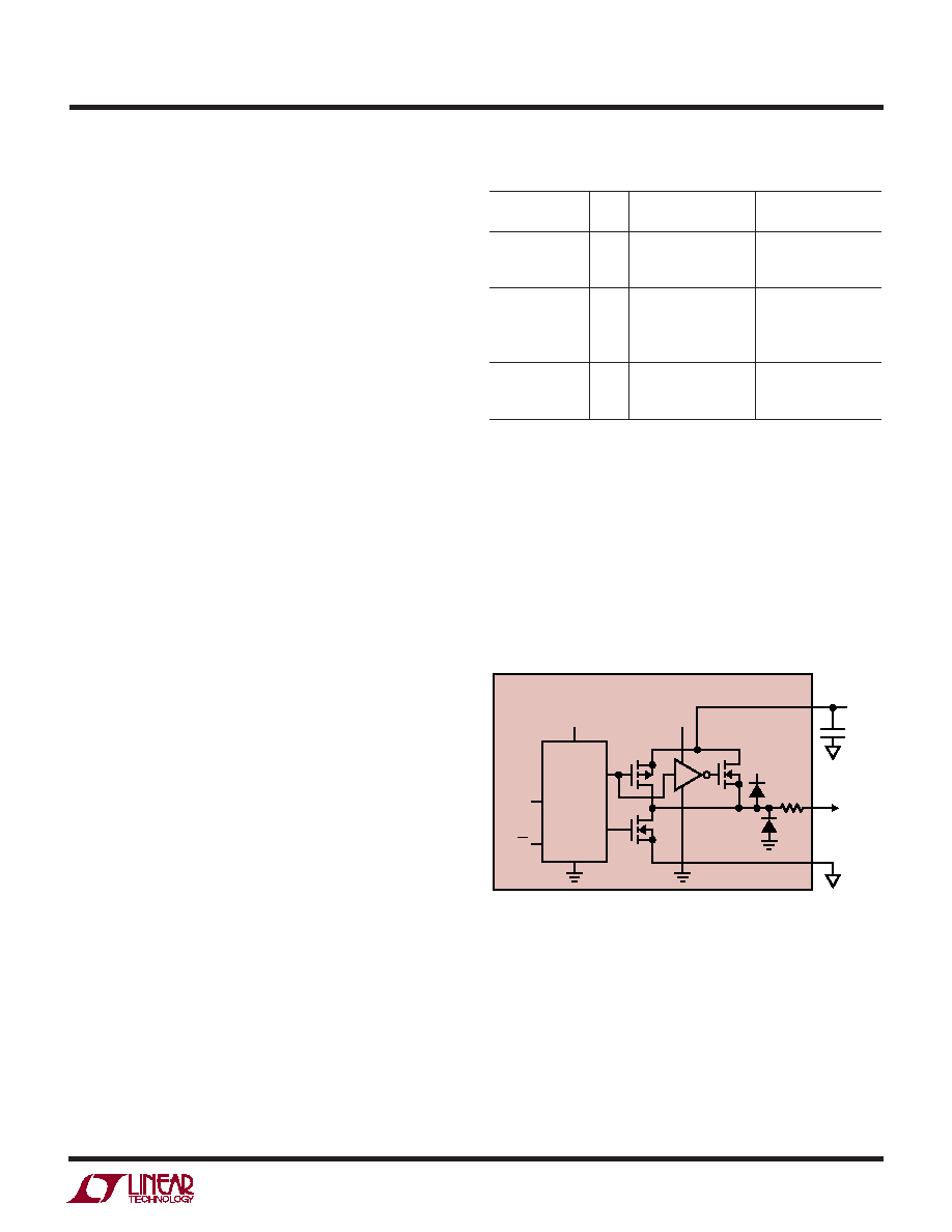
Digital Output Buffers
Figure 14 shows an equivalent circuit for a single output
buffer. Each buffer is powered by OVDD and OGND, iso-
lated from the ADC power and ground. The additional
N-channel transistor in the output driver allows operation
down to low voltages. The internal resistor in series with
the output makes the output appear as 50
to external
circuitry and may eliminate the need for external damping
resistors.
Table 1. Output Codes vs Input Voltage
AIN
+ – AIN–
D11 – D0
(2V Range)
OF
(Offset Binary)
(2’s Complement)
>+1.000000V
1
1111 1111 1111
0111 1111 1111
+0.999512V
0
1111 1111 1111
0111 1111 1111
+0.999024V
0
1111 1111 1110
0111 1111 1110
+0.000488V
0
1000 0000 0001
0000 0000 0001
0.000000V
0
1000 0000 0000
0000 0000 0000
–0.000488V
0
0111 1111 1111
1111 1111 1111
–0.000976V
0
0111 1111 1110
1111 1111 1110
–0.999512V
0
0000 0000 0001
1000 0000 0001
–1.000000V
0
0000 0000 0000
1000 0000 0000
<–1.000000V
1
0000 0000 0000
1000 0000 0000
229321 F14
OVDD
VDD
0.1
F
43
TYPICAL
DATA
OUTPUT
OGND
OVDD
0.5V
TO 3.6V
PREDRIVER
LOGIC
DATA
FROM
LATCH
OE
LTC2293/LTC2292/LTC2291
Figure 14. Digital Output Buffer
As with all high speed/high resolution converters, the digi-
tal output loading can affect the performance. The digital
outputs of the LTC2293/LTC2292/LTC2291 should drive a
minimal capacitive load to avoid possible interaction
between the digital outputs and sensitive input circuitry.
The output should be buffered with a device such as an
相关PDF资料 |
PDF描述 |
|---|---|
| AD7892ARZ-3 | IC ADC 12BIT LP 600KSPS 24SOIC |
| MS3100A20-6S | CONN RCPT 3POS WALL MNT W/SCKT |
| LTC2280IUP#PBF | IC ADC DUAL 10BIT 105MSPS 64-QFN |
| PT06A-14-5P | CONN PLUG 5 POS STRAIGHT W/PINS |
| TAS5615DKDR | IC AMP AUDIO 160W STER D 44HSSOP |
相关代理商/技术参数 |
参数描述 |
|---|---|
| LTC2291UP | 制造商:LINER 制造商全称:Linear Technology 功能描述:Dual 12-Bit, 65/40/25Msps Low Power 3V ADCs |
| LTC2292 | 制造商:LINER 制造商全称:Linear Technology 功能描述:Dual 12-Bit, 65/40/25Msps Low Power 3V ADCs |
| LTC2292CUP | 制造商:Linear Technology 功能描述:ADC Dual Pipelined 40Msps 12-bit Parallel 64-Pin QFN EP |
| LTC2292CUP#PBF | 功能描述:IC ADC DUAL 12BIT 40MSPS 64QFN RoHS:是 类别:集成电路 (IC) >> 数据采集 - 模数转换器 系列:- 其它有关文件:TSA1204 View All Specifications 标准包装:1 系列:- 位数:12 采样率(每秒):20M 数据接口:并联 转换器数目:2 功率耗散(最大):155mW 电压电源:模拟和数字 工作温度:-40°C ~ 85°C 安装类型:表面贴装 封装/外壳:48-TQFP 供应商设备封装:48-TQFP(7x7) 包装:Digi-Reel® 输入数目和类型:4 个单端,单极;2 个差分,单极 产品目录页面:1156 (CN2011-ZH PDF) 其它名称:497-5435-6 |
| LTC2292CUP#TRPBF | 功能描述:IC ADC DUAL 12BIT 40MSPS 64QFN RoHS:是 类别:集成电路 (IC) >> 数据采集 - 模数转换器 系列:- 标准包装:1,000 系列:- 位数:12 采样率(每秒):300k 数据接口:并联 转换器数目:1 功率耗散(最大):75mW 电压电源:单电源 工作温度:0°C ~ 70°C 安装类型:表面贴装 封装/外壳:24-SOIC(0.295",7.50mm 宽) 供应商设备封装:24-SOIC 包装:带卷 (TR) 输入数目和类型:1 个单端,单极;1 个单端,双极 |
发布紧急采购,3分钟左右您将得到回复。