参数资料
| 型号: | LTC2298IUP#PBF |
| 厂商: | Linear Technology |
| 文件页数: | 13/28页 |
| 文件大小: | 0K |
| 描述: | IC ADC DUAL 14BIT 65MSPS 64QFN |
| 标准包装: | 40 |
| 位数: | 14 |
| 采样率(每秒): | 65M |
| 数据接口: | 并联 |
| 转换器数目: | 2 |
| 功率耗散(最大): | 450mW |
| 电压电源: | 单电源 |
| 工作温度: | -40°C ~ 85°C |
| 安装类型: | 表面贴装 |
| 封装/外壳: | 64-WFQFN 裸露焊盘 |
| 供应商设备封装: | 64-QFN(9x9) |
| 包装: | 管件 |
| 输入数目和类型: | 2 个单端,双极; 2 个差分, 双极 |
第1页第2页第3页第4页第5页第6页第7页第8页第9页第10页第11页第12页当前第13页第14页第15页第16页第17页第18页第19页第20页第21页第22页第23页第24页第25页第26页第27页第28页
LTC2298/LTC2297/LTC2296
20
229876fa
CLK
5pF-30pF
ETC1-1T
0.1
F
VCM
FERRITE
BEAD
DIFFERENTIAL
CLOCK
INPUT
229876 F13
LTC2298
LTC2297
LTC2296
CLK
100
0.1
F
4.7
F
FERRITE
BEAD
CLEAN
SUPPLY
IF LVDS USE FIN1002 OR FIN1018.
FOR PECL, USE AZ1000ELT21 OR SIMILAR
229876 F12
LTC2298
LTC2297
LTC2296
APPLICATIO S I FOR ATIO
WU
UU
The noise performance of the LTC2298/LTC2297/LTC2296
can depend on the clock signal quality as much as on the
analog input. Any noise present on the clock signal will
result in additional aperture jitter that will be RMS summed
with the inherent ADC aperture jitter.
In applications where jitter is critical, such as when digitiz-
ing high input frequencies, use as large an amplitude as
possible. Also, if the ADC is clocked with a sinusoidal
signal, filter the CLK signal to reduce wideband noise and
distortion products generated by the source.
It is recommended that CLKA and CLKB are shorted
together and driven by the same clock source. If a small
time delay is desired between when the two channels
sample the analog inputs, CLKA and CLKB can be driven
by two different signals. If this delay exceeds 1ns, the
performance of the part may degrade. CLKA and CLKB
should not be driven by asynchronous signals.
Figures 12 and 13 show alternatives for converting a
differential clock to the single-ended CLK input. The use of
a transformer provides no incremental contribution to
phase noise. The LVDS or PECL to CMOS translators
provide little degradation below 70MHz, but at 140MHz
will degrade the SNR compared to the transformer solu-
tion. The nature of the received signals also has a large
bearing on how much SNR degradation will be experi-
enced. For high crest factor signals such as WCDMA or
OFDM, where the nominal power level must be at least 6dB
to 8dB below full scale, the use of these translators will
have a lesser impact.
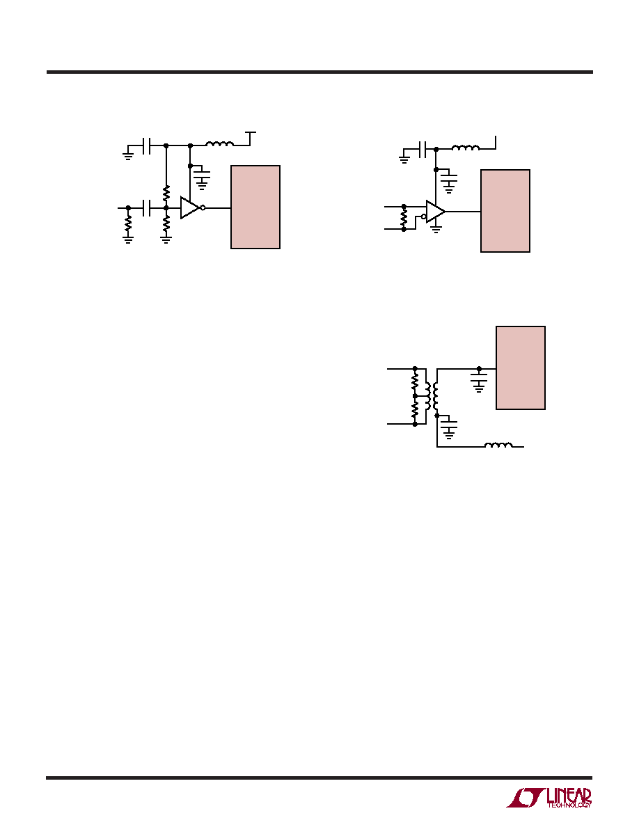
Figure 11. Sinusoidal Single-Ended CLK Drive
CLK
50
0.1
F
0.1
F
4.7
F
1k
FERRITE
BEAD
CLEAN
SUPPLY
SINUSOIDAL
CLOCK
INPUT
229876 F11
NC7SVU04
LTC2298
LTC2297
LTC2296
The transformer in the example may be terminated with
the appropriate termination for the signaling in use. The
use of a transformer with a 1:4 impedance ratio may be
desirable in cases where lower voltage differential signals
are considered. The center tap may be bypassed to
ground through a capacitor close to the ADC if the
differential signals originate on a different plane. The use
of a capacitor at the input may result in peaking, and
depending on transmission line length may require a 10
to 20
ohm series resistor to act as both a low pass filter
for high frequency noise that may be induced into the
clock line by neighboring digital signals, as well as a
damping mechanism for reflections.
Figure 13. LVDS or PECL CLK Drive Using a Transformer
Figure 12. CLK Drive Using an LVDS or PECL to CMOS Converter
相关PDF资料 |
PDF描述 |
|---|---|
| LTC2305CDE#TRPBF | IC ADC 12-BIT 2CHN 12-DFN |
| LTC2306CDD#PBF | IC ADC 12BIT 2CH 500KSPS 10-DFN |
| LTC2351HUH-12#TRPBF | IC ADC 12BIT 1.5MSPS 32-QFN |
| LTC2351HUH-14#TRPBF | IC ADC 14BIT 1.5MSPS 32-QFN |
| LTC2355IMSE-14#TRPBF | IC ADC 14BIT 3.5MSPS 10-MSOP |
相关代理商/技术参数 |
参数描述 |
|---|---|
| LTC2298UP | 制造商:LINER 制造商全称:Linear Technology 功能描述:Dual 14-Bit, 65/40/25Msps Low Power 3V ADCs |
| LTC2299 | 制造商:LINER 制造商全称:Linear Technology 功能描述:14-Bit, 125/105Msps Low Power 3V ADCs |
| LTC2299CUP | 制造商:LINER 制造商全称:Linear Technology 功能描述:Dual 14-Bit, 80Msps Low Power 3V ADC |
| LTC2299CUP#PBF | 功能描述:IC ADC DUAL 14BIT 80MSPS 64QFN RoHS:是 类别:集成电路 (IC) >> 数据采集 - 模数转换器 系列:- 标准包装:1 系列:microPOWER™ 位数:8 采样率(每秒):1M 数据接口:串行,SPI? 转换器数目:1 功率耗散(最大):- 电压电源:模拟和数字 工作温度:-40°C ~ 125°C 安装类型:表面贴装 封装/外壳:24-VFQFN 裸露焊盘 供应商设备封装:24-VQFN 裸露焊盘(4x4) 包装:Digi-Reel® 输入数目和类型:8 个单端,单极 产品目录页面:892 (CN2011-ZH PDF) 其它名称:296-25851-6 |
| LTC2299CUP#TRPBF | 功能描述:IC ADC DUAL 14BIT 80MSPS 64QFN RoHS:是 类别:集成电路 (IC) >> 数据采集 - 模数转换器 系列:- 标准包装:1 系列:- 位数:14 采样率(每秒):83k 数据接口:串行,并联 转换器数目:1 功率耗散(最大):95mW 电压电源:双 ± 工作温度:0°C ~ 70°C 安装类型:通孔 封装/外壳:28-DIP(0.600",15.24mm) 供应商设备封装:28-PDIP 包装:管件 输入数目和类型:1 个单端,双极 |
发布紧急采购,3分钟左右您将得到回复。