- 您现在的位置:买卖IC网 > PDF目录10511 > LTC2299IUP#PBF (Linear Technology)IC ADC DUAL 14BIT 80MSPS 64QFN PDF资料下载
参数资料
| 型号: | LTC2299IUP#PBF |
| 厂商: | Linear Technology |
| 文件页数: | 10/24页 |
| 文件大小: | 0K |
| 描述: | IC ADC DUAL 14BIT 80MSPS 64QFN |
| 标准包装: | 40 |
| 位数: | 14 |
| 采样率(每秒): | 80M |
| 数据接口: | 并联 |
| 转换器数目: | 2 |
| 功率耗散(最大): | 516mW |
| 电压电源: | 单电源 |
| 工作温度: | -40°C ~ 85°C |
| 安装类型: | 表面贴装 |
| 封装/外壳: | 64-WFQFN 裸露焊盘 |
| 供应商设备封装: | 64-QFN(9x9) |
| 包装: | 管件 |
| 输入数目和类型: | 2 个单端,双极; 2 个差分, 双极 |
LTC2299
2299fa
18
As with all high speed/high resolution converters, the
digital output loading can affect the performance. The
digital outputs of the LTC2299 should drive a minimal
capacitive load to avoid possible interaction between the
digital outputs and sensitive input circuitry. The output
should be buffered with a device such as an ALVCH16373
CMOS latch. For full speed operation the capacitive load
should be kept under 10pF.
Lower OVDD voltages will also help reduce interference
from the digital outputs.
Data Format
Using the MODE pin, the LTC2299 parallel digital output
can be selected for offset binary or 2’s complement
format. Note that MODE controls both Channel A and
Channel B. Connecting MODE to GND or 1/3VDD selects
offset binary output format. Connecting MODE to
2/3VDD or VDD selects 2’s complement output format. An
external resistor divider can be used to set the 1/3VDD or
2/3VDD logic values. Table 2 shows the logic states for the
MODE pin.
to 1V and must be less than OVDD. The logic outputs will
swing between OGND and OVDD.
Output Enable
The outputs may be disabled with the output enable pin, OE.
OE high disables all data outputs including OF. The data ac-
cess and bus relinquish times are too slow to allow the
outputs to be enabled and disabled during full speed op-
eration. The output Hi-Z state is intended for use during long
periods of inactivity. Channels A and B have independent
output enable pins (OEA, OEB).
Sleep and Nap Modes
The converter may be placed in shutdown or nap modes
to conserve power. Connecting SHDN to GND results in
normal operation. Connecting SHDN to VDD and OE to VDD
results in sleep mode, which powers down all circuitry
including the reference and typically dissipates 1mW. When
exiting sleep mode it will take milliseconds for the output
data to become valid because the reference capacitors have
to recharge and stabilize. Connecting SHDN to VDD and OE
to GND results in nap mode, which typically dissipates
30mW. In nap mode, the on-chip reference circuit is kept
on, so that recovery from nap mode is faster than that from
sleep mode, typically taking 100 clock cycles. In both sleep
and nap modes, all digital outputs are disabled and enter
the Hi-Z state.
Channels A and B have independent SHDN pins (SHDNA,
SHDNB). Channel A is controlled by SHDNA and OEA, and
Channel B is controlled by SHDNB and OEB. The nap, sleep
and output enable modes of the two channels are completely
independent, so it is possible to have one channel operat-
ing while the other channel is in nap or sleep mode.
Digital Output Multiplexer
The digital outputs of the LTC2299 can be multiplexed onto
a single data bus. The MUX pin is a digital input that swaps
the two data busses. If MUX is High, Channel A comes out
on DA0-DA13, OFA; Channel B comes out on DB0-DB13,
OFB. If MUX is Low, the output busses are swapped and
Channel A comes out on DB0-DB13, OFB; Channel B comes
out on DA0-DA13, OFA. To multiplex both channels onto
a single output bus, connect MUX, CLKA and CLKB together
APPLICATIO S I FOR ATIO
WU
U
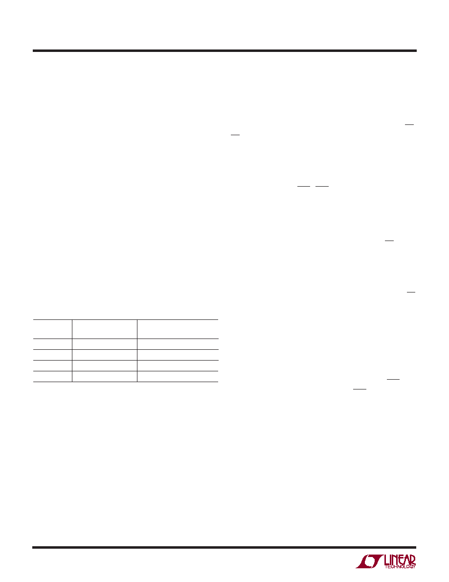
Table 2. MODE Pin Function
CLOCK DUTY
MODE PIN
OUTPUT FORMAT
CYCLE STABILIZER
0
Offset Binary
Off
1/3VDD
Offset Binary
On
2/3VDD
2’s Complement
On
VDD
2’s Complement
Off
Overflow Bit
When OF outputs a logic high the converter is either
overranged or underranged.
Output Driver Power
Separate output power and ground pins allow the output
drivers to be isolated from the analog circuitry. The power
supply for the digital output buffers, OVDD, should be tied
to the same power supply as for the logic being driven. For
example, if the converter is driving a DSP powered by a 1.8V
supply, then OVDD should be tied to that same 1.8V supply.
OVDD can be powered with any voltage from 500mV up to
3.6V. OGND can be powered with any voltage from GND up
相关PDF资料 |
PDF描述 |
|---|---|
| MAX1488EEPD+ | IC DVR RS232 QUAD 120KBPS 14-DIP |
| MAX13085EESA+ | IC TXRX RS485/422 8-SOIC |
| MS3102C24-10P | CONN RCPT 7POS BOX MNT W/PINS |
| MS3106A16S-4S | CONN PLUG 2POS STRAIGHT W/SCKT |
| MAX13053ESA+ | IC TRANSCEIVER CAN HS 8-SOIC |
相关代理商/技术参数 |
参数描述 |
|---|---|
| LTC2299UP | 制造商:LINER 制造商全称:Linear Technology 功能描述:Dual 14-Bit, 80Msps Low Power 3V ADC |
| LTC2301CDE#PBF | 功能描述:IC ADC 12BIT I2C 12-DFN RoHS:是 类别:集成电路 (IC) >> 数据采集 - 模数转换器 系列:- 其它有关文件:TSA1204 View All Specifications 标准包装:1 系列:- 位数:12 采样率(每秒):20M 数据接口:并联 转换器数目:2 功率耗散(最大):155mW 电压电源:模拟和数字 工作温度:-40°C ~ 85°C 安装类型:表面贴装 封装/外壳:48-TQFP 供应商设备封装:48-TQFP(7x7) 包装:Digi-Reel® 输入数目和类型:4 个单端,单极;2 个差分,单极 产品目录页面:1156 (CN2011-ZH PDF) 其它名称:497-5435-6 |
| LTC2301CDE#TRPBF | 功能描述:IC ADC 12-BIT 1CHN 12-DFN RoHS:是 类别:集成电路 (IC) >> 数据采集 - 模数转换器 系列:- 标准包装:2,500 系列:- 位数:16 采样率(每秒):15 数据接口:MICROWIRE?,串行,SPI? 转换器数目:1 功率耗散(最大):480µW 电压电源:单电源 工作温度:-40°C ~ 85°C 安装类型:表面贴装 封装/外壳:38-WFQFN 裸露焊盘 供应商设备封装:38-QFN(5x7) 包装:带卷 (TR) 输入数目和类型:16 个单端,双极;8 个差分,双极 配用:DC1011A-C-ND - BOARD DELTA SIGMA ADC LTC2494 |
| LTC2301CMS#PBF | 功能描述:IC ADC 12-BIT 1CHN 12-MSOP RoHS:是 类别:集成电路 (IC) >> 数据采集 - 模数转换器 系列:- 标准包装:2,500 系列:- 位数:16 采样率(每秒):15 数据接口:MICROWIRE?,串行,SPI? 转换器数目:1 功率耗散(最大):480µW 电压电源:单电源 工作温度:-40°C ~ 85°C 安装类型:表面贴装 封装/外壳:38-WFQFN 裸露焊盘 供应商设备封装:38-QFN(5x7) 包装:带卷 (TR) 输入数目和类型:16 个单端,双极;8 个差分,双极 配用:DC1011A-C-ND - BOARD DELTA SIGMA ADC LTC2494 |
| LTC2301CMS#TRPBF | 功能描述:IC ADC 12-BIT 1CHN 12-MSOP RoHS:是 类别:集成电路 (IC) >> 数据采集 - 模数转换器 系列:- 标准包装:2,500 系列:- 位数:16 采样率(每秒):15 数据接口:MICROWIRE?,串行,SPI? 转换器数目:1 功率耗散(最大):480µW 电压电源:单电源 工作温度:-40°C ~ 85°C 安装类型:表面贴装 封装/外壳:38-WFQFN 裸露焊盘 供应商设备封装:38-QFN(5x7) 包装:带卷 (TR) 输入数目和类型:16 个单端,双极;8 个差分,双极 配用:DC1011A-C-ND - BOARD DELTA SIGMA ADC LTC2494 |
发布紧急采购,3分钟左右您将得到回复。