- 您现在的位置:买卖IC网 > PDF目录10536 > LTC2351CUH-14#PBF (Linear Technology)IC ADC 14BIT 1.5MSPS 32-QFN PDF资料下载
参数资料
| 型号: | LTC2351CUH-14#PBF |
| 厂商: | Linear Technology |
| 文件页数: | 9/20页 |
| 文件大小: | 0K |
| 描述: | IC ADC 14BIT 1.5MSPS 32-QFN |
| 标准包装: | 73 |
| 位数: | 14 |
| 采样率(每秒): | 1.5M |
| 数据接口: | 串行,SPI? |
| 转换器数目: | 1 |
| 功率耗散(最大): | 16.5mW |
| 电压电源: | 单电源 |
| 工作温度: | 0°C ~ 70°C |
| 安装类型: | 表面贴装 |
| 封装/外壳: | 32-WFQFN 裸露焊盘 |
| 供应商设备封装: | 32-QFN 裸露焊盘(5x5) |
| 包装: | 管件 |
| 输入数目和类型: | 12 个单端,单极;12 个单端,双极;6 个差分,单极;6 个差分,双极 |
| 配用: | DC1278A-ND - BOARD SAR ADC LTC2351-14 |
LTC2351-14
17
235114fb
APPLICATIONS INFORMATION
and then buffer this signal with the appropriate number of
inverters to drive the serial clock input of the processor
serial port. Use the falling edge of the clock to latch data
from the serial data output (SDO) into your processor
serial port. The 14-bit serial data will be received in six
16-bit words with 96 or more clocks per frame sync. If
fewer than six channels are selected by SEL0–SEL2 for
conversion, then 16 clocks are needed per channel to
convert the analog inputs and read out the resulting data
after the next convert pulse. It is good practice to drive the
LTC2351-14 SCK input rst to avoid digital noise interfer-
ence during the internal bit comparison decision by the
internal high speed comparator. Unlike the CONV input,
the SCK input is not sensitive to jitter because the input
signal is already sampled and held constant.
Serial Data Output (SDO)
Upon power-up, the SDO output is automatically reset to
the high impedance state. The SDO output remains in high
impedance until a new conversion is started. SDO sends out
up to six sets of 14 bits in the output data stream after the
third rising edge of SCK after the start of conversion with
the rising edge of CONV. The six, or fewer, 14-bit words are
separated by two don’t care bits and two clock cycles in
high impedance mode. Please note the delay specication
from SCK to a valid SDO. SDO is always guaranteed to
be valid by the next rising edge of SCK. The 16- to 96-bit
output data stream is compatible with the 16-bit or 32-bit
serial port of most processors.
BOARD LAYOUT AND BYPASSING
Wire wrap boards are not recommended for high resolu-
tion and/or high speed A/D converters. To obtain the best
performance from the LTC2351-14, a printed circuit board
with ground plane is required. Layout for the printed circuit
board should ensure that digital and analog signal lines
are separated as much as possible. In particular, care
should be taken not to run any digital track alongside an
analog signal track. If optimum phase match between the
inputs is desired, the length of the twelve input wires of
the six input channels should be kept matched. But each
pair of input wires to the six input channels should be
kept separated by a ground trace to avoid high frequency
crosstalk between channels.
High quality tantalum and ceramic bypass capacitors
should be used at the VCC, VDD and VREF pins, as shown
in the Block Diagram on the rst page of this data sheet.
For optimum performance, a 10μF surface mount tantalum
capacitor with a 0.1μF ceramic is recommended for the
VCC, VDD and VREF pins. Alternatively, 10μF ceramic chip
capacitors such as X5R or X7R may be used. The capaci-
tors must be located as close to the pins as possible. The
traces connecting the pins and the bypass capacitors must
be kept short and should be made as wide as possible. The
VCC and VDD bypass capacitor returns to the ground plane
and the VREF bypass capacitor returns to the Pin 22. Care
should be taken to place the 0.1μF VCC and VDD bypass
capacitor as close to Pins 24 and 25 as possible.
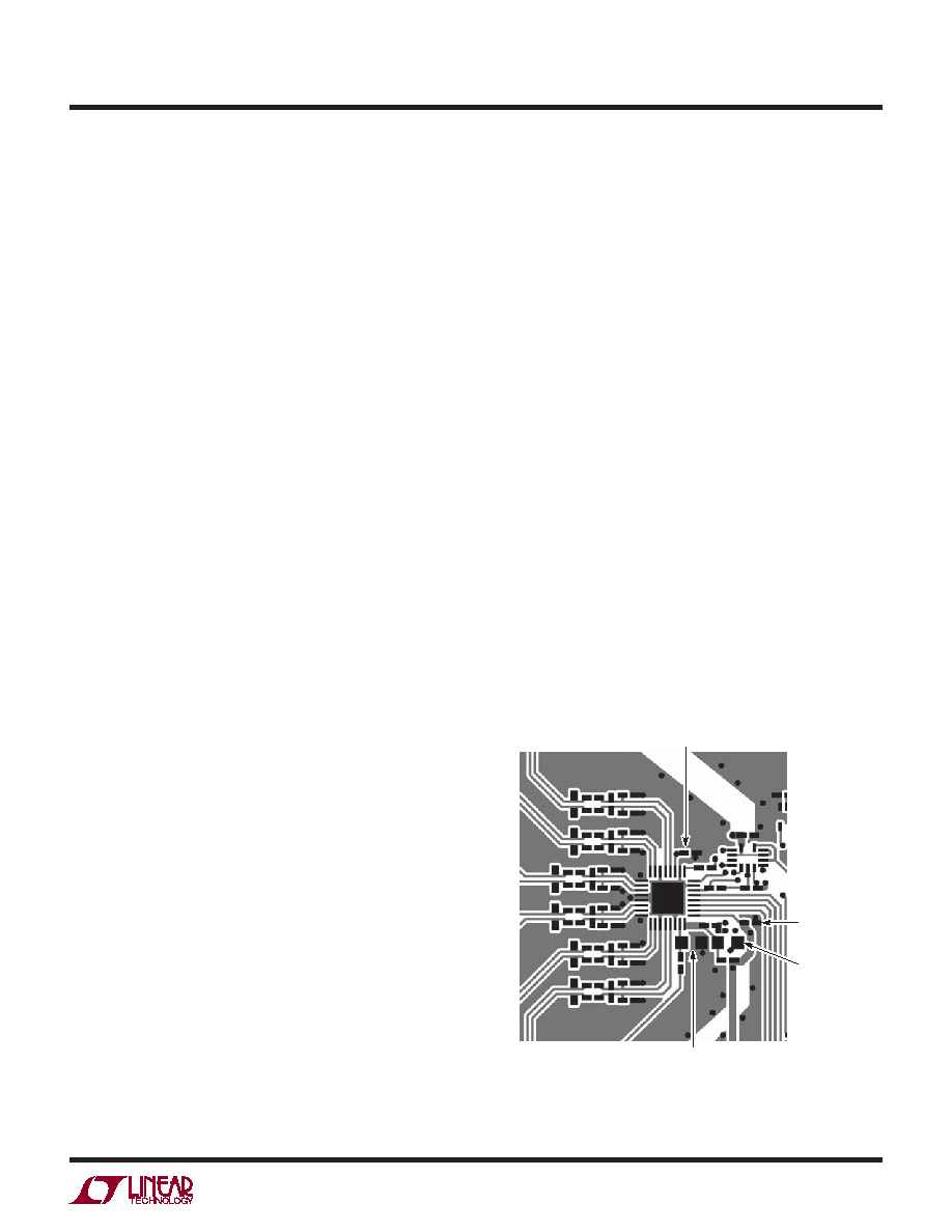
Figure 6 shows the recommended system ground connec-
tions. All analog circuitry grounds should be terminated at
the LTC2351-14 Exposed Pad. The ground return from the
LTC2351-14 to the power supply should be low impedance
for noise-free operation. The Exposed Pad of the 32-pin
QFN package is also internally tied to the ground pads.
The Exposed Pad should be soldered on the PC board to
reduce ground connection inductance. All ground pins
(GND, DGND, OGND) must be connected directly to the
same ground plane under the LTC2351-14.
VDD BYPASS,
0.1μF, 0402
OVDD BYPASS,
0.1μF, 0402
VREF BYPASS,
10μF, 0805
VCC BYPASS,
0.1μF, 0402 AND
10μF, 0805
235114 F06
Figure 6. Recommended Layout
相关PDF资料 |
PDF描述 |
|---|---|
| UMK105CK020CW-F | CAP CER 2PF 50V C0K 0402 |
| VE-J21-MY-F2 | CONVERTER MOD DC/DC 12V 50W |
| UMK105CK010DW-F | CAP CER 1PF 50V C0K 0402 |
| AD7856ARZ | IC ADC 14BIT 8CHAN 5V 24SOIC |
| VI-B44-MW | CONVERTER MOD DC/DC 48V 100W |
相关代理商/技术参数 |
参数描述 |
|---|---|
| LTC2351HUH-12#PBF | 功能描述:IC ADC 12BIT 1.5MSPS 32-QFN RoHS:是 类别:集成电路 (IC) >> 数据采集 - 模数转换器 系列:- 标准包装:1,000 系列:- 位数:12 采样率(每秒):300k 数据接口:并联 转换器数目:1 功率耗散(最大):75mW 电压电源:单电源 工作温度:0°C ~ 70°C 安装类型:表面贴装 封装/外壳:24-SOIC(0.295",7.50mm 宽) 供应商设备封装:24-SOIC 包装:带卷 (TR) 输入数目和类型:1 个单端,单极;1 个单端,双极 |
| LTC2351HUH-12#TRPBF | 功能描述:IC ADC 12BIT 1.5MSPS 32-QFN RoHS:是 类别:集成电路 (IC) >> 数据采集 - 模数转换器 系列:- 标准包装:1,000 系列:- 位数:12 采样率(每秒):300k 数据接口:并联 转换器数目:1 功率耗散(最大):75mW 电压电源:单电源 工作温度:0°C ~ 70°C 安装类型:表面贴装 封装/外壳:24-SOIC(0.295",7.50mm 宽) 供应商设备封装:24-SOIC 包装:带卷 (TR) 输入数目和类型:1 个单端,单极;1 个单端,双极 |
| LTC2351HUH-14#PBF | 功能描述:IC ADC 14BIT 1.5MSPS 32-QFN RoHS:是 类别:集成电路 (IC) >> 数据采集 - 模数转换器 系列:- 其它有关文件:TSA1204 View All Specifications 标准包装:1 系列:- 位数:12 采样率(每秒):20M 数据接口:并联 转换器数目:2 功率耗散(最大):155mW 电压电源:模拟和数字 工作温度:-40°C ~ 85°C 安装类型:表面贴装 封装/外壳:48-TQFP 供应商设备封装:48-TQFP(7x7) 包装:Digi-Reel® 输入数目和类型:4 个单端,单极;2 个差分,单极 产品目录页面:1156 (CN2011-ZH PDF) 其它名称:497-5435-6 |
| LTC2351HUH-14#TRPBF | 功能描述:IC ADC 14BIT 1.5MSPS 32-QFN RoHS:是 类别:集成电路 (IC) >> 数据采集 - 模数转换器 系列:- 标准包装:1,000 系列:- 位数:12 采样率(每秒):300k 数据接口:并联 转换器数目:1 功率耗散(最大):75mW 电压电源:单电源 工作温度:0°C ~ 70°C 安装类型:表面贴装 封装/外壳:24-SOIC(0.295",7.50mm 宽) 供应商设备封装:24-SOIC 包装:带卷 (TR) 输入数目和类型:1 个单端,单极;1 个单端,双极 |
| LTC2351IUH-12#PBF | 功能描述:IC ADC 12BIT 1.5MSPS 32-QFN RoHS:是 类别:集成电路 (IC) >> 数据采集 - 模数转换器 系列:- 标准包装:1,000 系列:- 位数:16 采样率(每秒):45k 数据接口:串行 转换器数目:2 功率耗散(最大):315mW 电压电源:模拟和数字 工作温度:0°C ~ 70°C 安装类型:表面贴装 封装/外壳:28-SOIC(0.295",7.50mm 宽) 供应商设备封装:28-SOIC W 包装:带卷 (TR) 输入数目和类型:2 个单端,单极 |
发布紧急采购,3分钟左右您将得到回复。