- 您现在的位置:买卖IC网 > PDF目录2006 > LTC2356IMSE-14#TRPBF (Linear Technology)IC ADC 14BIT 3.5MSPS 10-MSOP PDF资料下载
参数资料
| 型号: | LTC2356IMSE-14#TRPBF |
| 厂商: | Linear Technology |
| 文件页数: | 14/18页 |
| 文件大小: | 0K |
| 描述: | IC ADC 14BIT 3.5MSPS 10-MSOP |
| 标准包装: | 2,500 |
| 位数: | 14 |
| 采样率(每秒): | 3.5M |
| 数据接口: | 串行,SPI? |
| 转换器数目: | 1 |
| 功率耗散(最大): | 18mW |
| 电压电源: | 单电源 |
| 工作温度: | -40°C ~ 85°C |
| 安装类型: | 表面贴装 |
| 封装/外壳: | 10-TFSOP,10-MSOP(0.118",3.00mm 宽)裸露焊盘 |
| 供应商设备封装: | 10-MSOP 裸露焊盘 |
| 包装: | 带卷 (TR) |
| 输入数目和类型: | 2 个单端,双极;1 个差分,双极 |
| 配用: | DC1082A-E-ND - BOARD SAR ADC LTC2356-14 |
LTC2356-12/LTC2356-14
5
2356fb
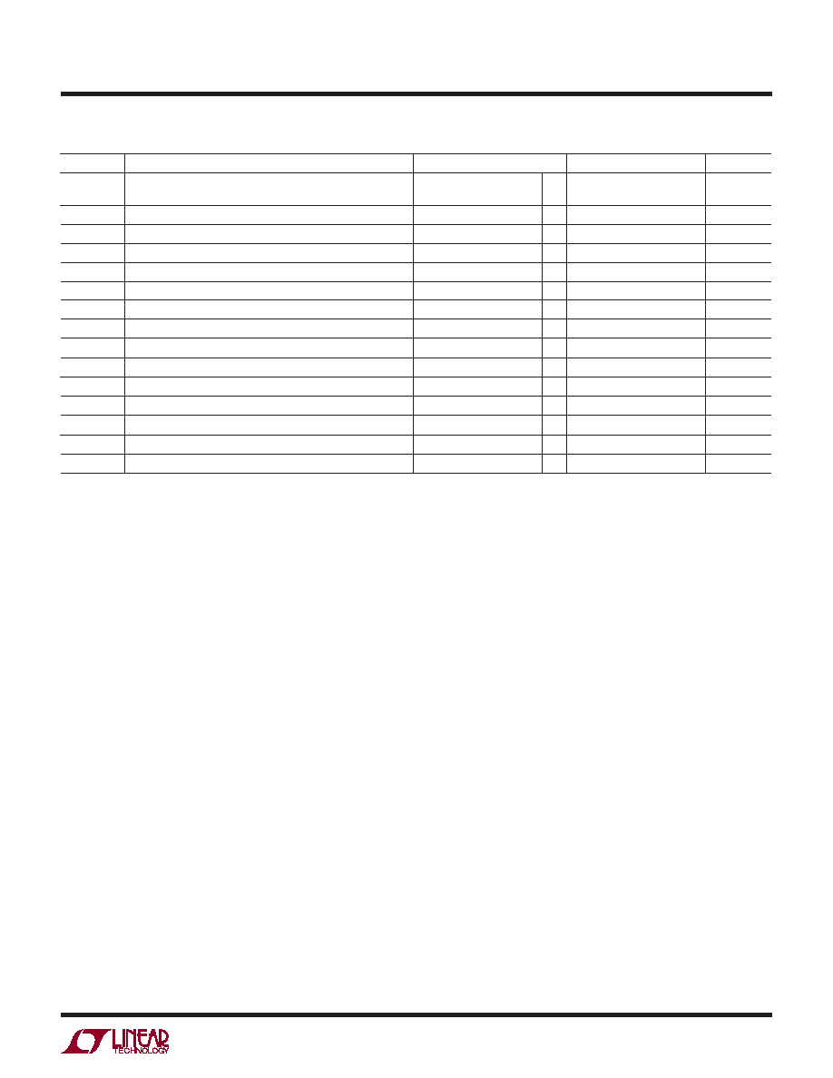
TIMING CHARACTERISTICS
Note 1: Stresses beyond those listed under Absolute Maximum Ratings
may cause permanent damage to the device. Exposure to any Absolute
Maximum Rating condition for extended periods may affect device
reliability and lifetime.
Note 2: All voltage values are with respect to GND.
Note 3: When these pins are taken below GND or above VDD, they will be
clamped by internal diodes. This product can handle input currents greater
than 100mA below GND or greater than VDD without latchup.
Note 4: Offset and full-gain specifications are measured for a single-ended
AIN+ input with AIN– grounded and using the internal 2.5V reference.
Note 5: Integral linearity is tested with an external 2.55V reference and is
defined as the deviation of a code from the straight line passing through
the actual endpoints of a transfer curve. The deviation is measured from
the center of quantization band.
Note 6: Guaranteed by design, not subject to test.
Note 7: Recommended operating conditions.
Note 8: The analog input range is defined for the voltage difference
between AIN+ and AIN–. Performance is specified with AIN– = 1.5V DC while
driving AIN+.
Note 9: The absolute voltage at AIN+ and AIN– must be within this range.
Note 10: If less than 3ns is allowed, the output data will appear one
clock cycle later. It is best for CONV to rise half a clock before SCK, when
running the clock at rated speed.
The l denotes the specifications which apply over the full operating temperature
range, otherwise specifications are at TA = 25°C. VDD = 3.3V.
SYMBOL
PARAMETER
CONDITIONS
MIN
TYP
MAX
UNITS
fSAMPLE(MAX) Maximum Sampling Rate per Channel
(Conversion Rate)
l
3.5
MHz
tTHROUGHPUT Minimum Sampling Period (Conversion + Acquisiton Period)
l
286
ns
tSCK
Clock Period
(Note 16)
l
15.872
10000
ns
tCONV
Conversion Time
(Note 6)
16
18
SCLK cycles
t1
Minimum High or Low SCLK Pulse Width
(Note 6)
2
ns
t2
CONV to SCK Setup Time
(Notes 6, 10)
3
ns
t3
Nearest SCK Edge Before CONV
(Note 6)
0
ns
t4
Minimum High or Low CONV Pulse Width
(Note 6)
4
ns
t5
SCK
↑ to Sample Mode
(Note 6)
4
ns
t6
CONV
↑ to Hold Mode
(Notes 6, 11)
1.2
ns
t7
16th SCK
↑ to CONV≠ Interval (Affects Acquisition Period)
(Notes 6, 7, 13)
45
ns
t8
Delay from SCK to Valid Data
(Notes 6, 12)
8
ns
t9
SCK
↑ to Hi-Z at SDO
(Notes 6, 12)
6
ns
t10
Previous SDO Bit Remains Valid After SCK
(Notes 6, 12)
2
ns
t12
VREF Settling Time After Sleep-to-Wake Transition
(Note 14)
2
ms
Note 11: Not the same as aperture delay. Aperture delay is smaller (1ns)
because the 2.2ns delay through the sample-and-hold is subtracted from
the CONV to Hold mode delay.
Note 12: The rising edge of SCK is guaranteed to catch the data coming
out into a storage latch.
Note 13: The time period for acquiring the input signal is started by the
16th rising clock and it is ended by the rising edge of convert.
Note 14: The internal reference settles in 2ms after it wakes up from Sleep
mode with one or more cycles at SCK and a 10F capacitive load.
Note 15: The full power bandwidth is the frequency where the output code
swing drops to 3dB with a 2.5VP-P input sine wave.
Note 16: Maximum clock period guarantees analog performance during
conversion. Output data can be read with an arbitrarily long clock.
Note 17: VDD = 3.3V, fSAMPLE = 3.5Msps.
Note 18: The LTC2356-14 is measured and specified with 14-bit resolution
(1LSB = 152V) and the LTC2356-12 is measured and specified with
12-bit resolution (1LSB = 610V).
Note 19: The sampling capacitor at each input accounts for 4.1pF of the
input capacitance.
相关PDF资料 |
PDF描述 |
|---|---|
| LTC2366HTS8#TRPBF | IC ADC 12BIT 3MSPS TSOT23-8 |
| LTC2379HMS-18#PBF | IC ADC 18BIT SPI/SRL 16MSOP |
| LTC2380HMS-16#TRPBF | IC ADC 16BIT 2MSPS 16-MSOP |
| LTC2382HMS-16#PBF | IC ADC 16BIT 1CH 500KSPS 16-MSOP |
| LTC2383HMS-16#PBF | IC ADC 16BIT 1CH 1MSPS 16-MSOP |
相关代理商/技术参数 |
参数描述 |
|---|---|
| LTC2360CS6#TRMPBF | 功能描述:IC ADC 12BIT 100KSPS TSOT23-6 RoHS:是 类别:集成电路 (IC) >> 数据采集 - 模数转换器 系列:- 标准包装:2,500 系列:- 位数:16 采样率(每秒):15 数据接口:MICROWIRE?,串行,SPI? 转换器数目:1 功率耗散(最大):480µW 电压电源:单电源 工作温度:-40°C ~ 85°C 安装类型:表面贴装 封装/外壳:38-WFQFN 裸露焊盘 供应商设备封装:38-QFN(5x7) 包装:带卷 (TR) 输入数目和类型:16 个单端,双极;8 个差分,双极 配用:DC1011A-C-ND - BOARD DELTA SIGMA ADC LTC2494 |
| LTC2360CS6#TRPBF | 功能描述:IC ADC 12BIT 100KSPS TSOT23-6 RoHS:是 类别:集成电路 (IC) >> 数据采集 - 模数转换器 系列:- 标准包装:2,500 系列:- 位数:16 采样率(每秒):15 数据接口:MICROWIRE?,串行,SPI? 转换器数目:1 功率耗散(最大):480µW 电压电源:单电源 工作温度:-40°C ~ 85°C 安装类型:表面贴装 封装/外壳:38-WFQFN 裸露焊盘 供应商设备封装:38-QFN(5x7) 包装:带卷 (TR) 输入数目和类型:16 个单端,双极;8 个差分,双极 配用:DC1011A-C-ND - BOARD DELTA SIGMA ADC LTC2494 |
| LTC2360CTS8#TRMPBF | 功能描述:IC ADC 12BIT 100KSPS TSOT23-8 RoHS:是 类别:集成电路 (IC) >> 数据采集 - 模数转换器 系列:- 标准包装:2,500 系列:- 位数:16 采样率(每秒):15 数据接口:MICROWIRE?,串行,SPI? 转换器数目:1 功率耗散(最大):480µW 电压电源:单电源 工作温度:-40°C ~ 85°C 安装类型:表面贴装 封装/外壳:38-WFQFN 裸露焊盘 供应商设备封装:38-QFN(5x7) 包装:带卷 (TR) 输入数目和类型:16 个单端,双极;8 个差分,双极 配用:DC1011A-C-ND - BOARD DELTA SIGMA ADC LTC2494 |
| LTC2360CTS8#TRPBF | 功能描述:IC ADC 12BIT 100KSPS TSOT23-8 RoHS:是 类别:集成电路 (IC) >> 数据采集 - 模数转换器 系列:- 标准包装:2,500 系列:- 位数:16 采样率(每秒):15 数据接口:MICROWIRE?,串行,SPI? 转换器数目:1 功率耗散(最大):480µW 电压电源:单电源 工作温度:-40°C ~ 85°C 安装类型:表面贴装 封装/外壳:38-WFQFN 裸露焊盘 供应商设备封装:38-QFN(5x7) 包装:带卷 (TR) 输入数目和类型:16 个单端,双极;8 个差分,双极 配用:DC1011A-C-ND - BOARD DELTA SIGMA ADC LTC2494 |
| LTC2360HS6#PBF | 制造商:Linear Technology 功能描述:MS-ADC/General Purpose, Cut Tape 12-bit 100ksps SAR ADC in TSOT-6 |
发布紧急采购,3分钟左右您将得到回复。