- 您现在的位置:买卖IC网 > PDF目录10567 > LTC2366ITS8#TRMPBF (Linear Technology)IC ADC 12BIT 3MSPS TSOT23-8 PDF资料下载
参数资料
| 型号: | LTC2366ITS8#TRMPBF |
| 厂商: | Linear Technology |
| 文件页数: | 6/24页 |
| 文件大小: | 0K |
| 描述: | IC ADC 12BIT 3MSPS TSOT23-8 |
| 标准包装: | 1 |
| 位数: | 12 |
| 采样率(每秒): | 3M |
| 数据接口: | MICROWIRE?,串行,SPI? |
| 转换器数目: | 1 |
| 功率耗散(最大): | 14.4mW |
| 电压电源: | 单电源 |
| 工作温度: | -40°C ~ 85°C |
| 安装类型: | 表面贴装 |
| 封装/外壳: | SOT-23-8 薄型,TSOT-23-8 |
| 供应商设备封装: | TSOT-23-8 |
| 包装: | 标准包装 |
| 输入数目和类型: | 1 个单端,单极 |
| 产品目录页面: | 1347 (CN2011-ZH PDF) |
| 其它名称: | LTC2366ITS8#TRMPBFDKR |
LTC2365/LTC2366
14
23656fb
For more information www.linear.com/LTC2365
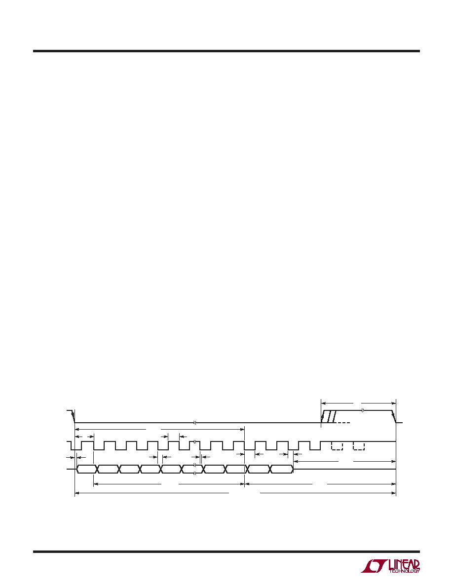
Figure 10. LTC2365/LTC2366 Serial Interface Timing Diagram
applications inForMation
OVERVIEW
The LTC2365/LTC2366 use a successive approximation
algorithm and internal sample-and-hold circuit to convert
an analog signal to a 12-bit serial output. Both devices
operate from a single 2.35V to 3.6V supply. The LTC2366
samples at a rate of 3Msps with a 48MHz clock while the
LTC2365 samples at a rate of 1Msps with a 16MHz clock.
TheLTC2365/LTC2366containa12-bit,switched-capacitor
ADC, a sample-and-hold, and a serial interface (see Block
Diagram) and are available in tiny 6- and 8-lead TSOT-23
packages.Thedevicesprovidesleepmodecontrolthrough
the serial interface to save power during inactive periods
(see the SLEEP MODE section).
The S6 package of the LTC2365/LTC2366 uses VDD as the
reference and has an analog input range of 0V to VDD. The
ADC samples the analog input with respect to GND and
outputs the result through the serial interface.
The TS8 package provides two additional pins: a reference
input pin, VREF, and an output supply pin, OVDD. The ADC
can operate with reduced spans down to 1.4V and achieve
342V resolution. OVDD controls the output swing of the
digital output pin, SDO, and allows the device to com-
municate with 1.8V, 2.5V or 3V digital systems.
SERIAL INTERFACE
The LTC2365/LTC2366 communicate with microcon-
trollers, DSPs and other external circuitry via a 3-wire
interface. Figure 10 shows the serial interface timing dia-
gram, while Figures 11 and 12 detail the timing diagrams
ofconversioncyclesin14and16SCKcycles,respectively.
Data Transfer
A falling CS edge starts a conversion and frames the se-
rial data transfer. SCK provides the conversion clock and
controls the data transfer during the conversion.
CS going LOW clocks out the first leading zero and sub-
sequent SCK falling edges clock out the remaining data,
beginning with the second leading zero. (Therefore, the
first SCK falling edge captures the first leading zero and
clocks out the second leading zero). The timing diagram
in Figure 12 shows that the final bit in the data transfer is
valid on the 16th falling edge, since it is clocked out on
the previous 15th falling edge.
In applications with a slower SCK, it is possible to capture
data on each SCK rising edge. In such cases, the first
falling edge of SCK clocks out the second leading zero
and can be captured on the first rising edge. However,
the first leading zero clocked out when CS goes LOW is
missed, as shown in Figures 11 and 12. In Figure 12, the
15th falling edge of SCK clocks out the last bit and can
be captured on the 15th rising SCK edge.
If CS goes LOW while SCK is LOW, then CS clocks out the
first leading zero and can be captured on the SCK rising
edge. The next SCK falling edge clocks out the second
leading zero and can be captured on the following rising
edge, as shown in Figure 10.
1
SCK
SDO
t2
t3
t4
t7
t5
t8
ZERO
B11
B10
B9
B1
B0
ZERO
2
3
4
(MSB)
Hi-Z STATE
5
13
14
15
16
t6
tQUIET
tACQ
13tSCK
tTHROUGHPUT
tCONV
CS
t1
23656 F10
相关PDF资料 |
PDF描述 |
|---|---|
| VI-J0K-MY-F1 | CONVERTER MOD DC/DC 40V 50W |
| VI-J0J-MY-F4 | CONVERTER MOD DC/DC 36V 50W |
| VI-J0L-MY-F1 | CONVERTER MOD DC/DC 28V 50W |
| 205841-2 | CONN RECEPT CPC 8POS STD SER 2 |
| VI-J0K-MY-F4 | CONVERTER MOD DC/DC 40V 50W |
相关代理商/技术参数 |
参数描述 |
|---|---|
| LTC2367CDE-16#PBF | 功能描述:IC ADC 16BIT SPI/SRL 500K 16-DFN RoHS:是 类别:集成电路 (IC) >> 数据采集 - 模数转换器 系列:- 标准包装:1 系列:- 位数:14 采样率(每秒):83k 数据接口:串行,并联 转换器数目:1 功率耗散(最大):95mW 电压电源:双 ± 工作温度:0°C ~ 70°C 安装类型:通孔 封装/外壳:28-DIP(0.600",15.24mm) 供应商设备封装:28-PDIP 包装:管件 输入数目和类型:1 个单端,双极 |
| LTC2367CDE-16#TRPBF | 功能描述:IC ADC 16BIT SPI/SRL 500K 16-DFN RoHS:是 类别:集成电路 (IC) >> 数据采集 - 模数转换器 系列:- 标准包装:1 系列:- 位数:14 采样率(每秒):83k 数据接口:串行,并联 转换器数目:1 功率耗散(最大):95mW 电压电源:双 ± 工作温度:0°C ~ 70°C 安装类型:通孔 封装/外壳:28-DIP(0.600",15.24mm) 供应商设备封装:28-PDIP 包装:管件 输入数目和类型:1 个单端,双极 |
| LTC2367CDE-18#PBF | 功能描述:IC ADC 18BIT SPI/SRL 500K 16DFN RoHS:是 类别:集成电路 (IC) >> 数据采集 - 模数转换器 系列:- 其它有关文件:TSA1204 View All Specifications 标准包装:1 系列:- 位数:12 采样率(每秒):20M 数据接口:并联 转换器数目:2 功率耗散(最大):155mW 电压电源:模拟和数字 工作温度:-40°C ~ 85°C 安装类型:表面贴装 封装/外壳:48-TQFP 供应商设备封装:48-TQFP(7x7) 包装:Digi-Reel® 输入数目和类型:4 个单端,单极;2 个差分,单极 产品目录页面:1156 (CN2011-ZH PDF) 其它名称:497-5435-6 |
| LTC2367CDE-18#TRPBF | 功能描述:IC ADC 18BIT 500K 1CH 16DFN RoHS:是 类别:集成电路 (IC) >> 数据采集 - 模数转换器 系列:- 标准包装:1 系列:- 位数:14 采样率(每秒):83k 数据接口:串行,并联 转换器数目:1 功率耗散(最大):95mW 电压电源:双 ± 工作温度:0°C ~ 70°C 安装类型:通孔 封装/外壳:28-DIP(0.600",15.24mm) 供应商设备封装:28-PDIP 包装:管件 输入数目和类型:1 个单端,双极 |
| LTC2367CMS-16#PBF | 功能描述:IC ADC 16BIT SPI/SRL 500K 16MSOP RoHS:是 类别:集成电路 (IC) >> 数据采集 - 模数转换器 系列:- 其它有关文件:TSA1204 View All Specifications 标准包装:1 系列:- 位数:12 采样率(每秒):20M 数据接口:并联 转换器数目:2 功率耗散(最大):155mW 电压电源:模拟和数字 工作温度:-40°C ~ 85°C 安装类型:表面贴装 封装/外壳:48-TQFP 供应商设备封装:48-TQFP(7x7) 包装:Digi-Reel® 输入数目和类型:4 个单端,单极;2 个差分,单极 产品目录页面:1156 (CN2011-ZH PDF) 其它名称:497-5435-6 |
发布紧急采购,3分钟左右您将得到回复。