- 您现在的位置:买卖IC网 > PDF目录39417 > LTC2376IMS-16#TRPBF (LINEAR TECHNOLOGY CORP) 1-CH 16-BIT SUCCESSIVE APPROXIMATION ADC, SERIAL ACCESS, PDSO16 PDF资料下载
参数资料
| 型号: | LTC2376IMS-16#TRPBF |
| 厂商: | LINEAR TECHNOLOGY CORP |
| 元件分类: | ADC |
| 英文描述: | 1-CH 16-BIT SUCCESSIVE APPROXIMATION ADC, SERIAL ACCESS, PDSO16 |
| 封装: | LEAD FREE, PLASTIC, MSOP-16 |
| 文件页数: | 6/24页 |
| 文件大小: | 2229K |
| 代理商: | LTC2376IMS-16#TRPBF |
LTC2376-16
14
237616f
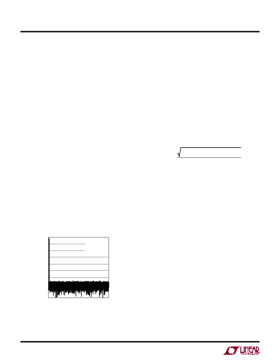
Figure 11. 32k Point FFT with fIN = 2kHz of the LTC2376-16
FREQUENCY (kHz)
0
25
125
100
75
50
–180
AMPLITUDE
(dBFS)
–60
–40
–20
–80
–100
–120
–140
–160
0
237616 F11
SNR = 97.1dB
THD = –125dB
SINAD = 97.1dB
SFDR = 128dB
applicaTions inForMaTion
0A to a maximum of 0.2mA at 250ksps. This step in DC
current draw triggers a transient response in the reference
that must be considered since any deviation in the refer-
ence output voltage will affect the accuracy of the output
code. In applications where the transient response of the
reference is important, the fast settling LTC6655-5 refer-
ence is also recommended.
DYNAMIC PERFORMANCE
Fast Fourier Transform (FFT) techniques are used to test
the ADC’s frequency response, distortion and noise at the
rated throughput. By applying a low distortion sine wave
and analyzing the digital output using an FFT algorithm,
the ADC’s spectral content can be examined for frequen-
cies outside the fundamental. The LTC2376-16 provides
guaranteed tested limits for both AC distortion and noise
measurements.
Signal-to-Noise and Distortion Ratio (SINAD)
The signal-to-noise and distortion ratio (SINAD) is the
ratio between the RMS amplitude of the fundamental input
frequency and the RMS amplitude of all other frequency
components at the A/D output. The output is band-limited
to frequencies from above DC and below half the sampling
frequency. Figure 11 shows that the LTC2376-16 achieves
a typical SINAD of 97dB at a 250kHz sampling rate with
a 2kHz input.
Signal-to-Noise Ratio (SNR)
The signal-to-noise ratio (SNR) is the ratio between the
RMS amplitude of the fundamental input frequency and
the RMS amplitude of all other frequency components
except the first five harmonics and DC. Figure 11 shows
that the LTC2376-16 achieves a typical SNR of 97dB at a
250kHz sampling rate with a 2kHz input.
Total Harmonic Distortion (THD)
TotalHarmonicDistortion(THD)istheratiooftheRMSsum
ofallharmonicsoftheinputsignaltothefundamentalitself.
The out-of-band harmonics alias into the frequency band
between DC and half the sampling frequency (fSMPL/2).
THD is expressed as:
THD
=20log
V22
+ V32 + V42 +…+ VN
2
V1
where V1 is the RMS amplitude of the fundamental fre-
quencyandV2throughVNaretheamplitudesofthesecond
through Nth harmonics.
POWER CONSIDERATIONS
The LTC2376-16 provides two power supply pins: the
2.5V power supply (VDD), and the digital input/output
interface power supply (OVDD). The flexible OVDD supply
allows the LTC2376-16 to communicate with any digital
logic operating between 1.8V and 5V, including 2.5V and
3.3V systems.
Power Supply Sequencing
The LTC2376-16 does not have any specific power supply
sequencing requirements. Care should be taken to adhere
to the maximum voltage relationships described in the
Absolute Maximum Ratings section. The LTC2376-16
has a power-on-reset (POR) circuit that will reset the
LTC2376-16 at initial power-up or whenever the power
supply voltage drops below 1V. Once the supply voltage
re-enters the nominal supply voltage range, the POR will
reinitialize the ADC. No conversions should be initiated
until 20s after a POR event to ensure the reinitialization
period has ended. Any conversions initiated before this
time will produce invalid results.
相关PDF资料 |
PDF描述 |
|---|---|
| LTC2376HMS-16#TRPBF | 1-CH 16-BIT SUCCESSIVE APPROXIMATION ADC, SERIAL ACCESS, PDSO16 |
| LTC2376IMS-16#PBF | 1-CH 16-BIT SUCCESSIVE APPROXIMATION ADC, SERIAL ACCESS, PDSO16 |
| LTC2376IDE-16#TRPBF | 1-CH 16-BIT SUCCESSIVE APPROXIMATION ADC, SERIAL ACCESS, PDSO16 |
| LTC2376CMS-16#TRPBF | 1-CH 16-BIT SUCCESSIVE APPROXIMATION ADC, SERIAL ACCESS, PDSO16 |
| LTC2376HMS-16#PBF | 1-CH 16-BIT SUCCESSIVE APPROXIMATION ADC, SERIAL ACCESS, PDSO16 |
相关代理商/技术参数 |
参数描述 |
|---|---|
| LTC2376IMS-18#PBF | 功能描述:IC ADC 18BIT 250KSPS 16-MSOP RoHS:是 类别:集成电路 (IC) >> 数据采集 - 模数转换器 系列:- 其它有关文件:TSA1204 View All Specifications 标准包装:1 系列:- 位数:12 采样率(每秒):20M 数据接口:并联 转换器数目:2 功率耗散(最大):155mW 电压电源:模拟和数字 工作温度:-40°C ~ 85°C 安装类型:表面贴装 封装/外壳:48-TQFP 供应商设备封装:48-TQFP(7x7) 包装:Digi-Reel® 输入数目和类型:4 个单端,单极;2 个差分,单极 产品目录页面:1156 (CN2011-ZH PDF) 其它名称:497-5435-6 |
| LTC2376IMS-18#TRPBF | 功能描述:IC ADC 18BIT 250KSPS 16-MSOP RoHS:是 类别:集成电路 (IC) >> 数据采集 - 模数转换器 系列:- 标准包装:1 系列:- 位数:14 采样率(每秒):83k 数据接口:串行,并联 转换器数目:1 功率耗散(最大):95mW 电压电源:双 ± 工作温度:0°C ~ 70°C 安装类型:通孔 封装/外壳:28-DIP(0.600",15.24mm) 供应商设备封装:28-PDIP 包装:管件 输入数目和类型:1 个单端,双极 |
| LTC2376IMS-20#PBF | 制造商:Linear Technology 功能描述:IC ADC 20BIT 250KSPS 16MSOP |
| LTC2376IMS-20#PBF | 制造商:Linear Technology 功能描述:ADC 20BIT 250KSPS SPI MSOP-16 |
| LTC2376IMS-20#TRPBF | 制造商:Linear Technology 功能描述:IC ADC 20BIT 250KSPS 16MSOP |
发布紧急采购,3分钟左右您将得到回复。