- 您现在的位置:买卖IC网 > PDF目录10092 > LTC2380IDE-16#TRPBF (Linear Technology)IC ADC 16BIT 2MSPS 16-DFN PDF资料下载
参数资料
| 型号: | LTC2380IDE-16#TRPBF |
| 厂商: | Linear Technology |
| 文件页数: | 3/26页 |
| 文件大小: | 0K |
| 描述: | IC ADC 16BIT 2MSPS 16-DFN |
| 产品培训模块: | LTC2379- 18-/16-bit Fully-Differential SAR ADC Family Overview |
| 标准包装: | 2,500 |
| 位数: | 16 |
| 采样率(每秒): | 2M |
| 数据接口: | 串行,SPI? |
| 转换器数目: | 1 |
| 功率耗散(最大): | 22mW |
| 电压电源: | 模拟和数字 |
| 工作温度: | -40°C ~ 85°C |
| 安装类型: | 表面贴装 |
| 封装/外壳: | 16-WFDFN 裸露焊盘 |
| 供应商设备封装: | 16-DFN(4x3) |
| 包装: | 带卷 (TR) |
| 输入数目和类型: | * |
| 配用: | DC1783A-A-ND - BOARD SAR ADC LTC2380-16 |
LTC2380-16
11
238016fa
APPLICATIONS INFORMATION
INPUT DRIVE CIRCUITS
A low impedance source can directly drive the high im-
pedance inputs of the LTC2380-16 without gain error. A
high impedance source should be buffered to minimize
settling time during acquisition and to optimize the dis-
tortion performance of the ADC. Minimizing settling time
is important even for DC inputs, because the ADC inputs
draw a current spike when entering acquisition.
For best performance, a buffer amplifier should be used
to drive the analog inputs of the LTC2380-16. The ampli-
fier provides low output impedance, which produces fast
settling of the analog signal during the acquisition phase.
It also provides isolation between the signal source and
the current spike the ADC inputs draw.
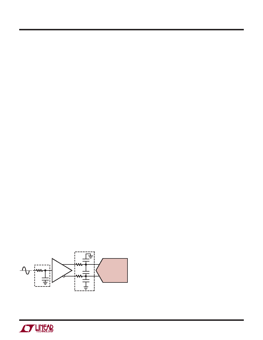
Input Filtering
The noise and distortion of the buffer amplifier and signal
source must be considered since they add to the ADC noise
and distortion. Noisy input signals should be filtered prior
to the buffer amplifier input with an appropriate filter to
minimize noise. The simple 1-pole RC lowpass filter (LPF1)
shown in Figure 4 is sufficient for many applications.
Another filter network consisting of LPF2 should be used
between the buffer and ADC input to both minimize the
noise contribution of the buffer and to help minimize distur-
bances reflected into the buffer from sampling transients.
Long RC time constants at the analog inputs will slow
down the settling of the analog inputs. Therefore, LPF2
requires a wider bandwidth than LPF1. A buffer amplifier
with a low noise density must be selected to minimize
degradation of the SNR.
20Ω
3300pF
6600pF
20Ω
500Ω
LPF2
LPF1
BW = 800kHz
BW = 48kHz
SINGLE-ENDED-
TO-DIFFERENTIAL
DRIVER
SINGLE-ENDED-
INPUT SIGNAL
LTC2380-16
IN+
IN–
238016 F04
3300pF
High quality capacitors and resistors should be used in the
RC filters since these components can add distortion. NPO
and silver mica type dielectric capacitors have excellent
linearity. Carbon surface mount resistors can generate
distortion from self heating and from damage that may
occur during soldering. Metal film surface mount resistors
are much less susceptible to both problems.
Single-Ended-to-Differential Conversion
For single-ended input signals, a single-ended to differential
conversion circuit must be used to produce a differential
signal at the inputs of the LTC2380-16. The LT6350 ADC
driver is recommended for performing single-ended-to-
differential conversions. The LT6350 is flexible and may
be configured to convert single-ended signals of various
amplitudes to the ±5V differential input range of the
LTC2380-16. The LT6350 is also available in H-grade to
complement the extended temperature operation of the
LTC2380-16 up to 125°C.
Figure 5a shows the LT6350 being used to convert a 0V
to 5V single-ended input signal. In this case, the first
amplifier is configured as a unity gain buffer and the single-
ended input signal directly drives the high-impedance
input of the amplifier. As shown in the FFT of Figure 5b,
the LT6350 drives the LTC2380-16 to near full datasheet
performance.
The LT6350 can also be used to buffer and convert large
true bipolar signals which swing below ground to the
±5V differential input range of the LTC2380-16 in order
to maximize the signal swing that can be digitized. Fig-
ure6a shows the LT6350 being used to convert a ±10V
true bipolar signal for use by the LTC2380-16. In this
case, the first amplifier in the LT6350 is configured as
an inverting amplifier stage, which acts to attenuate and
level shift the input signal to the 0V to 5V input range of
the LTC2380-16. In the inverting amplifier configuration,
the single-ended input signal source no longer directly
drives a high impedance input of the first amplifier. The
input impedance is instead set by resistor RIN. RIN must
be chosen carefully based on the source impedance of the
signal source. Higher values of RIN tend to degrade both
the noise and distortion of the LT6350 and LTC2380-16
as a system.
Figure 4. Input Signal Chain
相关PDF资料 |
PDF描述 |
|---|---|
| IDT72V221L10J8 | IC FIFO SYNC 1KX9 10NS 32PLCC |
| MS27484P8A35S | CONN PLUG 6POS STRAIGHT W/SCKT |
| VI-B33-IV-F4 | CONVERTER MOD DC/DC 24V 150W |
| IDT72V215L15PFI8 | IC FIFO SYNC 512X18 15NS 64-TQFP |
| MS3102C28-6SW | CONN RCPT 3POS BOX MNT W/SCKT |
相关代理商/技术参数 |
参数描述 |
|---|---|
| LTC2380IMS-16#PBF | 功能描述:IC ADC 16BIT 2MSPS 16-MSOP RoHS:是 类别:集成电路 (IC) >> 数据采集 - 模数转换器 系列:- 其它有关文件:TSA1204 View All Specifications 标准包装:1 系列:- 位数:12 采样率(每秒):20M 数据接口:并联 转换器数目:2 功率耗散(最大):155mW 电压电源:模拟和数字 工作温度:-40°C ~ 85°C 安装类型:表面贴装 封装/外壳:48-TQFP 供应商设备封装:48-TQFP(7x7) 包装:Digi-Reel® 输入数目和类型:4 个单端,单极;2 个差分,单极 产品目录页面:1156 (CN2011-ZH PDF) 其它名称:497-5435-6 |
| LTC2380IMS-16#PBF-ES | 制造商:Linear Technology 功能描述:ADC Single SAR 2Msps 16-bit Serial 16-Pin MSOP |
| LTC2380IMS-16#TRPBF | 功能描述:IC ADC 16BIT 2MSPS 16-MSOP RoHS:是 类别:集成电路 (IC) >> 数据采集 - 模数转换器 系列:- 标准包装:1 系列:- 位数:14 采样率(每秒):83k 数据接口:串行,并联 转换器数目:1 功率耗散(最大):95mW 电压电源:双 ± 工作温度:0°C ~ 70°C 安装类型:通孔 封装/外壳:28-DIP(0.600",15.24mm) 供应商设备封装:28-PDIP 包装:管件 输入数目和类型:1 个单端,双极 |
| LTC2380IMS-16#TRPBF-ES | 制造商:Linear Technology 功能描述:ADC Single SAR 2Msps 16-bit Serial 16-Pin MSOP T/R |
| LTC2381CDE-16#PBF | 功能描述:IC ADC 16BIT 1CH 250KSPS 16-DFN RoHS:是 类别:集成电路 (IC) >> 数据采集 - 模数转换器 系列:- 标准包装:1,000 系列:- 位数:16 采样率(每秒):45k 数据接口:串行 转换器数目:2 功率耗散(最大):315mW 电压电源:模拟和数字 工作温度:0°C ~ 70°C 安装类型:表面贴装 封装/外壳:28-SOIC(0.295",7.50mm 宽) 供应商设备封装:28-SOIC W 包装:带卷 (TR) 输入数目和类型:2 个单端,单极 |
发布紧急采购,3分钟左右您将得到回复。