- 您现在的位置:买卖IC网 > PDF目录10245 > LTC2391CLX-16#PBF (Linear Technology)IC ADC 16BIT SER/PAR 250K 48LQFP PDF资料下载
参数资料
| 型号: | LTC2391CLX-16#PBF |
| 厂商: | Linear Technology |
| 文件页数: | 7/24页 |
| 文件大小: | 0K |
| 描述: | IC ADC 16BIT SER/PAR 250K 48LQFP |
| 标准包装: | 250 |
| 位数: | 16 |
| 采样率(每秒): | 250k |
| 数据接口: | 串行,并联 |
| 转换器数目: | 1 |
| 功率耗散(最大): | 125mW |
| 电压电源: | 模拟和数字 |
| 工作温度: | 0°C ~ 70°C |
| 安装类型: | 表面贴装 |
| 封装/外壳: | 48-LQFP |
| 供应商设备封装: | 48-LQFP(7x7) |
| 包装: | 托盘 |
| 输入数目和类型: | 1 个差分,双极 |
| 配用: | DC1500A-C-ND - BOARD SAR ADC LTC2391-16 |
LTC2391-16
15
239116fa
APPLICATIONS INFORMATION
= low is applied. In this mode, power consumption drops
to a typical value of 175μW from 95mW. This mode can
be used if the LTC2391-16 is inactive for a long period of
time and the user wants to minimize the power dissipation.
Recovery from Power Shutdown Mode
Once the PD pin is returned to a low level, ending the
power shutdown request, the internal circuitry will begin
to power up. If the internal reference is used, the 2.6kΩ
output impedance with the 1μF bypass capacitor on the
REFIN/REFOUT pins will be the main time constant for
the power-on recovery time. If an external reference is
used, typically allow 5ms for recovery before initiating a
new conversion.
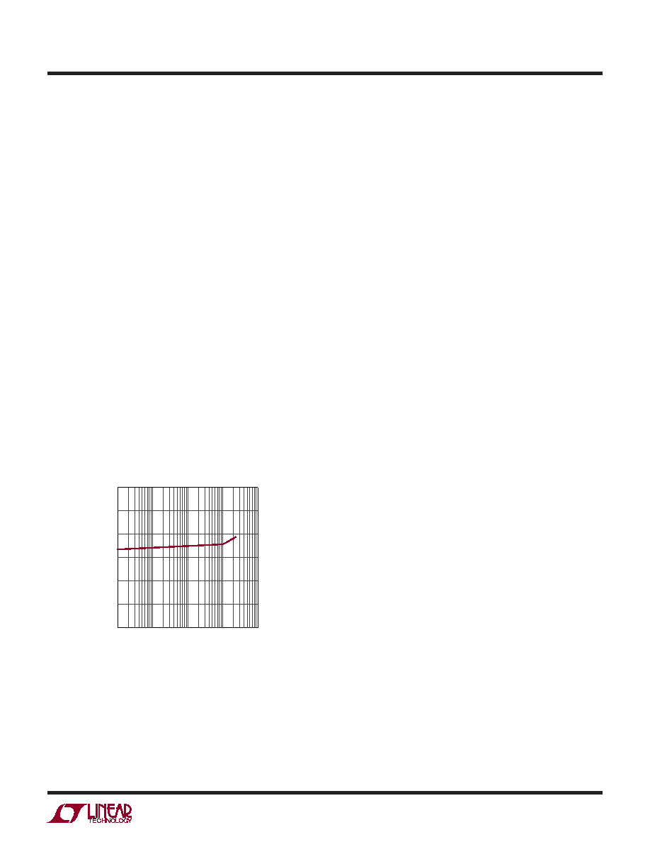
Power Dissipation vs Sampling Frequency
The power dissipation of the LTC2391-16 will decrease
as the sampling frequency is reduced when nap mode
is activated. See Figure 7. In nap mode, a portion of the
circuitry on the LTC2391-16 is turned off after a conversion
has been completed. Increasing the time allowed between
conversions lowers the average power.
TIMING AND CONTROL
The LTC2391-16 conversion is controlled by CNVST. A
falling edge on CNVST will start a conversion. CS and RD
control the digital interface on the LTC2391-16. When
either CS or RD is high, the digital outputs are high
impedance.
CNVST Timing
The LTC2391-16 conversion is controlled by CNVST. A
falling edge on CNVST will start a conversion. Once a
conversion has been initiated, it cannot be restarted until
the conversion is complete. For optimum performance
CNVST should be a clean low jitter signal. Converter status
is indicated by the BUSY output which remains high while
the conversion is in progress. To ensure no errors occur
in the digitized results return the rising edge either within
40ns from the start of the conversion or wait until after
the conversion has been completed. The CNVST timing
needed to take advantage of the reduced power mode of
operation is described in the Nap Mode section.
Internal Conversion Clock
The LTC2391-16 has an internal clock that is trimmed
to achieve a maximum conversion time of 2500ns. No
external adjustments are required and with a maximum
acquisition time of 1485ns, a throughput performance of
250ksps is guaranteed.
DIGITAL INTERFACE
The LTC2391-16 allows both parallel and serial digital
interfaces. The exible OVP supply allows the LTC2391-16
to communicate with any digital logic operating between
1.8V and 5V, including 2.5V and 3.3V systems.
Figure 7. Power Dissipation of the LTC2391-16
Decreases with Decreasing Sampling Frequency
SAMPLING FREQUENCY (kHz)
10
POWER
SUPPL
Y
CURRENT
(mA)
20
30
5
15
25
0.1
10
100
1000
239116 G15
0
1
相关PDF资料 |
PDF描述 |
|---|---|
| NE570DG | IC COMPANDOR DUAL GAIN 16-SOIC |
| MS27473E10A35PB | CONN PLUG 13POS STRAIGHT W/PINS |
| LTC2391CUK-16#PBF | IC ADC 16BIT SER/PAR 250K 48QFN |
| LTC1418IG#TR | IC A/D CONV 14BIT SRL&PAR 28SSOP |
| MS3106F24-9P | CONN PLUG 2POS STRAIGHT W/PINS |
相关代理商/技术参数 |
参数描述 |
|---|---|
| LTC2391CUK-16#PBF | 功能描述:IC ADC 16BIT SER/PAR 250K 48QFN RoHS:是 类别:集成电路 (IC) >> 数据采集 - 模数转换器 系列:- 标准包装:1,000 系列:- 位数:12 采样率(每秒):300k 数据接口:并联 转换器数目:1 功率耗散(最大):75mW 电压电源:单电源 工作温度:0°C ~ 70°C 安装类型:表面贴装 封装/外壳:24-SOIC(0.295",7.50mm 宽) 供应商设备封装:24-SOIC 包装:带卷 (TR) 输入数目和类型:1 个单端,单极;1 个单端,双极 |
| LTC2391CUK-16#PBF | 制造商:Linear Technology 功能描述:ANALOG TO DIGITAL (A/D) CONVERTER IC |
| LTC2391CUK-16#TRPBF | 功能描述:IC ADC 16BIT SER/PAR 250K 48QFN RoHS:是 类别:集成电路 (IC) >> 数据采集 - 模数转换器 系列:- 标准包装:1,000 系列:- 位数:12 采样率(每秒):300k 数据接口:并联 转换器数目:1 功率耗散(最大):75mW 电压电源:单电源 工作温度:0°C ~ 70°C 安装类型:表面贴装 封装/外壳:24-SOIC(0.295",7.50mm 宽) 供应商设备封装:24-SOIC 包装:带卷 (TR) 输入数目和类型:1 个单端,单极;1 个单端,双极 |
| LTC2391HLX-16#PBF | 功能描述:IC ADC 16B SER/PAR 250K 48LQFP RoHS:是 类别:集成电路 (IC) >> 数据采集 - 模数转换器 系列:- 标准包装:1,000 系列:- 位数:12 采样率(每秒):300k 数据接口:并联 转换器数目:1 功率耗散(最大):75mW 电压电源:单电源 工作温度:0°C ~ 70°C 安装类型:表面贴装 封装/外壳:24-SOIC(0.295",7.50mm 宽) 供应商设备封装:24-SOIC 包装:带卷 (TR) 输入数目和类型:1 个单端,单极;1 个单端,双极 |
| LTC2391ILX-16#PBF | 功能描述:IC ADC 16B SER/PAR 250K 48LQFP RoHS:是 类别:集成电路 (IC) >> 数据采集 - 模数转换器 系列:- 标准包装:1,000 系列:- 位数:12 采样率(每秒):300k 数据接口:并联 转换器数目:1 功率耗散(最大):75mW 电压电源:单电源 工作温度:0°C ~ 70°C 安装类型:表面贴装 封装/外壳:24-SOIC(0.295",7.50mm 宽) 供应商设备封装:24-SOIC 包装:带卷 (TR) 输入数目和类型:1 个单端,单极;1 个单端,双极 |
发布紧急采购,3分钟左右您将得到回复。