- 您现在的位置:买卖IC网 > PDF目录10300 > LTC2410CGN (Linear Technology)IC ADC 24BIT DIFF INP/REF 16SSOP PDF资料下载
参数资料
| 型号: | LTC2410CGN |
| 厂商: | Linear Technology |
| 文件页数: | 31/48页 |
| 文件大小: | 0K |
| 描述: | IC ADC 24BIT DIFF INP/REF 16SSOP |
| 标准包装: | 100 |
| 位数: | 24 |
| 采样率(每秒): | 7.5 |
| 数据接口: | MICROWIRE?,串行,SPI? |
| 转换器数目: | 2 |
| 功率耗散(最大): | 1mW |
| 电压电源: | 单电源 |
| 工作温度: | 0°C ~ 70°C |
| 安装类型: | 表面贴装 |
| 封装/外壳: | 16-SSOP(0.154",3.90mm 宽) |
| 供应商设备封装: | 16-SSOP |
| 包装: | 管件 |
| 输入数目和类型: | 1 个差分,双极 |
| 配用: | DC575A-ND - BOARD DELTA SIGMA ADC LTC2410 |
| 其它名称: | Q894257 |
第1页第2页第3页第4页第5页第6页第7页第8页第9页第10页第11页第12页第13页第14页第15页第16页第17页第18页第19页第20页第21页第22页第23页第24页第25页第26页第27页第28页第29页第30页当前第31页第32页第33页第34页第35页第36页第37页第38页第39页第40页第41页第42页第43页第44页第45页第46页第47页第48页
LTC2410
37
APPLICATIO S I FOR ATIO
WU
U
techniques is used to produce a precision divide operation
on the reference signal. Another option is the use of a
reference within the 5V input range of the LTC2410 and
developing excitation via fixed gain, or LTC1043 based
voltage multiplication, along with remote feedback in the
excitation amplifiers, as shown in Figures 52 and 53.
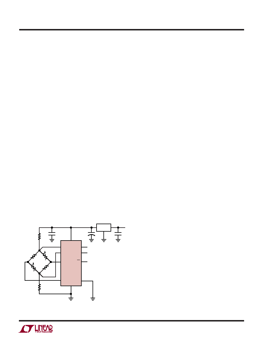
Figure 47 shows an example of a simple bridge connec-
tion. Note that it is suitable for any bridge application
where measurement speed is not of the utmost impor-
tance. For many applications where large vessels are
weighed, the average weight over an extended period of
time is of concern and short term weight is not readily
determined due to movement of contents, or mechanical
resonance. Often, large weighing applications involve load
cells located at each load bearing point, the output of
which can be summed passively prior to the signal pro-
cessing circuitry, actively with amplification prior to the
ADC, or can be digitized via multiple ADC channels and
summed mathematically. The mathematical summation
of the output of multiple LTC2410’s provides the benefit of
a root square reduction in noise. The low power consump-
tion of the LTC2410 makes it attractive for multidrop
communication schemes where the ADC is located within
the load-cell housing.
A direct connection to a load cell is perhaps best incorpo-
rated into the load-cell body, as minimizing the distance to
the sensor largely eliminates the need for protection
devices, RFI suppression and wiring. The LTC2410 exhib-
its extremely low temperature dependent drift. As a result,
exposure to external ambient temperature ranges does
not compromise performance. The incorporation of any
amplification considerably complicates thermal stability,
as input offset voltages and currents, temperature coeffi-
cient of gain settling resistors all become factors.
The circuit in Figure 48 shows an example of a simple
amplification scheme. This example produces a differen-
tial output with a common mode voltage of 2.5V, as
determined by the bridge. The use of a true three amplifier
instrumentation amplifier is not necessary, as the LTC2410
has common mode rejection far beyond that of most
amplifiers. The LTC1051 is a dual autozero amplifier that
can be used to produce a gain of 15 before its input
referred noise dominates the LTC2410 noise. This ex-
ample shows a gain of 34, that is determined by a feedback
network built using a resistor array containing 8 individual
resistors. The resistors are organized to optimize tem-
perature tracking in the presence of thermal gradients. The
second LTC1051 buffers the low noise input stage from
the transient load steps produced during conversion.
The gain stability and accuracy of this approach is very
good, due to a statistical improvement in resistor match-
ing. A gain of 34 may seem low, when compared to
common practice in earlier generations of load-cell inter-
faces, however the accuracy of the LTC2410 changes the
rationale. Achieving high gain accuracy and linearity at
higher gains may prove difficult, while providing little
benefit in terms of noise reduction.
At a gain of 100, the gain error that could result from
typical open-loop gain of 160dB is –1ppm, however,
worst-case is at the minimum gain of 116dB, giving a gain
error of –158ppm. Worst-case gain error at a gain of 34,
is –54ppm. The use of the LTC1051A reduces the worst-
case gain error to –33ppm. The advantage of gain higher
than 34, then becomes dubious, as the input referred
noise sees little improvement1 and gain accuracy is poten-
tially compromised.
Note that this 4-amplifier topology has advantages over
the typical integrated 3-amplifier instrumentation ampli-
fier in that it does not have the high noise level common in
the output stage that usually dominates when an instru-
Figure 47. Simple Bridge Connection
REF+
REF–
SDO
SCK
IN+
IN–
CS
GND
VREF
FO
3
R1
12
4
350
BRIDGE
13
5
6
2410 F47
11
1, 7, 8, 9,
10, 15, 16
2
14
LTC2410
+
R2
R1 AND R2 CAN BE USED TO INCREASE TOLERABLE AC COMPONENT ON REF SIGNALS
LT1019
相关PDF资料 |
PDF描述 |
|---|---|
| LTC1594CS#TRPBF | IC A/D CONV 12BIT SRL 4CH 16SOIC |
| LTC1594CS#TR | IC ADC 12BIT 5V 4CH SAMPL 16SOIC |
| LTC1594LCS#TRPBF | IC A/D CONV 12BIT SRL 4CH 16SOIC |
| MS27473E10A13S | CONN PLUG 13POS STRAIGHT W/SCKT |
| LTC1594LCS#TR | IC ADC 12BIT 3V 4CH SAMPL 16SOIC |
相关代理商/技术参数 |
参数描述 |
|---|---|
| LTC2410CGN#PBF | 功能描述:IC ADC 24BIT DIFF INP/REF 16SSOP RoHS:是 类别:集成电路 (IC) >> 数据采集 - 模数转换器 系列:- 标准包装:1 系列:microPOWER™ 位数:8 采样率(每秒):1M 数据接口:串行,SPI? 转换器数目:1 功率耗散(最大):- 电压电源:模拟和数字 工作温度:-40°C ~ 125°C 安装类型:表面贴装 封装/外壳:24-VFQFN 裸露焊盘 供应商设备封装:24-VQFN 裸露焊盘(4x4) 包装:Digi-Reel® 输入数目和类型:8 个单端,单极 产品目录页面:892 (CN2011-ZH PDF) 其它名称:296-25851-6 |
| LTC2410CGN#PBF | 制造商:Linear Technology 功能描述:A/D Converter (A-D) IC |
| LTC2410CGN#TR | 功能描述:IC ADC 24BIT DIFF INP/REF 16SSOP RoHS:否 类别:集成电路 (IC) >> 数据采集 - 模数转换器 系列:- 标准包装:1,000 系列:- 位数:16 采样率(每秒):45k 数据接口:串行 转换器数目:2 功率耗散(最大):315mW 电压电源:模拟和数字 工作温度:0°C ~ 70°C 安装类型:表面贴装 封装/外壳:28-SOIC(0.295",7.50mm 宽) 供应商设备封装:28-SOIC W 包装:带卷 (TR) 输入数目和类型:2 个单端,单极 |
| LTC2410CGN#TRPBF | 功能描述:IC ADC 24BIT DIFF INP/REF 16SSOP RoHS:是 类别:集成电路 (IC) >> 数据采集 - 模数转换器 系列:- 标准包装:1,000 系列:- 位数:16 采样率(每秒):45k 数据接口:串行 转换器数目:2 功率耗散(最大):315mW 电压电源:模拟和数字 工作温度:0°C ~ 70°C 安装类型:表面贴装 封装/外壳:28-SOIC(0.295",7.50mm 宽) 供应商设备封装:28-SOIC W 包装:带卷 (TR) 输入数目和类型:2 个单端,单极 |
| LTC2410CGNPBF | 制造商:Linear Technology 功能描述:ADC,LTC2410C 24bit diff D-S SPI SSOP |
发布紧急采购,3分钟左右您将得到回复。