- 您现在的位置:买卖IC网 > PDF目录10672 > LTC2410IGN#PBF (Linear Technology)IC ADC 24BIT DIFF INP/REF 16SSOP PDF资料下载
参数资料
| 型号: | LTC2410IGN#PBF |
| 厂商: | Linear Technology |
| 文件页数: | 5/48页 |
| 文件大小: | 0K |
| 描述: | IC ADC 24BIT DIFF INP/REF 16SSOP |
| 标准包装: | 100 |
| 位数: | 24 |
| 采样率(每秒): | 7.5 |
| 数据接口: | MICROWIRE?,串行,SPI? |
| 转换器数目: | 2 |
| 功率耗散(最大): | 1mW |
| 电压电源: | 单电源 |
| 工作温度: | -40°C ~ 85°C |
| 安装类型: | 表面贴装 |
| 封装/外壳: | 16-SSOP(0.154",3.90mm 宽) |
| 供应商设备封装: | 16-SSOP |
| 包装: | 管件 |
| 输入数目和类型: | 1 个差分,双极 |
| 配用: | DC575A-ND - BOARD DELTA SIGMA ADC LTC2410 |
第1页第2页第3页第4页当前第5页第6页第7页第8页第9页第10页第11页第12页第13页第14页第15页第16页第17页第18页第19页第20页第21页第22页第23页第24页第25页第26页第27页第28页第29页第30页第31页第32页第33页第34页第35页第36页第37页第38页第39页第40页第41页第42页第43页第44页第45页第46页第47页第48页
LTC2410
13
Input Voltage Range
The analog input is truly differential with an absolute/
common mode range for the IN+ and IN– input pins
extending from GND – 0.3V to VCC + 0.3V. Outside
these limits, the ESD protection devices begin to turn on
and the errors due to input leakage current increase
rapidly. Within these limits, the LTC2410 converts the
bipolar differential input signal, VIN = IN+ – IN–, from
– FS = – 0.5 VREF to +FS = 0.5 VREF where VREF =
REF+ – REF–. Outside this range, the converter indicates
the overrange or the underrange condition using distinct
output codes.
Input signals applied to IN+ and IN– pins may extend by
300mV below ground and above VCC. In order to limit any
fault current, resistors of up to 5k may be added in series
with the IN+ and IN– pins without affecting the perfor-
mance of the device. In the physical layout, it is important
to maintain the parasitic capacitance of the connection
between these series resistors and the corresponding pins
as low as possible; therefore, the resistors should be
located as close as practical to the pins. The effect of the
series resistance on the converter accuracy can be evalu-
ated from the curves presented in the Input Current/
Reference Current sections. In addition, series resistors
will introduce a temperature dependent offset error due to
the input leakage current. A 1nA input leakage current will
develop a 1ppm offset error on a 5k resistor if VREF = 5V.
This error has a very strong temperature dependency.
Output Data Format
The LTC2410 serial output data stream is 32 bits long. The
first 3 bits represent status information indicating the sign
and conversion state. The next 24 bits are the conversion
result, MSB first. The remaining 5 bits are sub LSBs
beyond the 24-bit level that may be included in averaging
or discarded without loss of resolution. The third and
fourth bit together are also used to indicate an underrange
condition (the differential input voltage is below –FS) or an
overrange condition (the differential input voltage is above
+FS).
Bit 31 (first output bit) is the end of conversion (EOC)
indicator. This bit is available at the SDO pin during the
conversion and sleep states whenever the CS pin is LOW.
This bit is HIGH during the conversion and goes LOW
when the conversion is complete.
Bit 30 (second output bit) is a dummy bit (DMY) and is
always LOW.
Bit 29 (third output bit) is the conversion result sign indi-
cator (SIG). If VIN is >0, this bit is HIGH. If VIN is <0, this
bit is LOW.
Bit 28 (fourth output bit) is the most significant bit (MSB)
of the result. This bit in conjunction with Bit 29 also
provides the underrange or overrange indication. If both
Bit 29 and Bit 28 are HIGH, the differential input voltage is
above +FS. If both Bit 29 and Bit 28 are LOW, the
differential input voltage is below –FS.
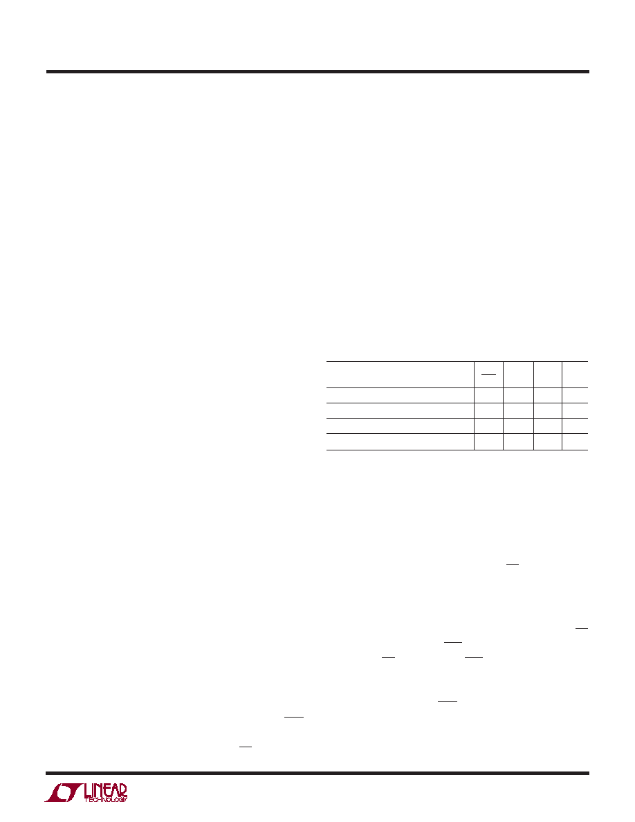
The function of these bits is summarized in Table 1.
Table 1. LTC2410 Status Bits
Bit 31
Bit 30 Bit 29 Bit 28
Input Range
EOC
DMY
SIG
MSB
VIN ≥ 0.5 VREF
00
1
0V
≤ VIN < 0.5 VREF
00
1
0
–0.5 VREF ≤ VIN < 0V
0
1
VIN < – 0.5 VREF
00
0
Bits 28-5 are the 24-bit conversion result MSB first.
Bit 5 is the least significant bit (LSB).
Bits 4-0 are sub LSBs below the 24-bit level. Bits 4-0 may
be included in averaging or discarded without loss of
resolution.
Data is shifted out of the SDO pin under control of the serial
clock (SCK), see Figure 3. Whenever CS is HIGH, SDO
remains high impedance and any externally generated
SCK clock pulses are ignored by the internal data out shift
register.
In order to shift the conversion result out of the device, CS
must first be driven LOW. EOC is seen at the SDO pin of the
device once CS is pulled LOW. EOC changes real time from
HIGH to LOW at the completion of a conversion. This
signal may be used as an interrupt for an external
microcontroller. Bit 31 (EOC) can be captured on the first
rising edge of SCK. Bit 30 is shifted out of the device on the
first falling edge of SCK. The final data bit (Bit 0) is shifted
out on the falling edge of the 31st SCK and may be latched
APPLICATIO S I FOR ATIO
WU
U
相关PDF资料 |
PDF描述 |
|---|---|
| AD7680BRMZ | IC ADC 16BIT LP UNIPOLAR 8-MSOP |
| AD7472ARUZ | IC ADC 12BIT PAR 1.5MSPS 24TSSOP |
| ISL3333IRZ | IC TXRX RS485/422 2PRT 40-QFN |
| LTC1594IS#PBF | IC A/D CONV 12BIT SRL 4CH 16SOIC |
| ISL81334IAZ | IC TXRX DUAL 2PORT ESD 28-SSOP |
相关代理商/技术参数 |
参数描述 |
|---|---|
| LTC2411-1CMS | 功能描述:IC A/DCONV DIFF INPUT&REF 10MSOP RoHS:否 类别:集成电路 (IC) >> 数据采集 - 模数转换器 系列:- 标准包装:1,000 系列:- 位数:16 采样率(每秒):45k 数据接口:串行 转换器数目:2 功率耗散(最大):315mW 电压电源:模拟和数字 工作温度:0°C ~ 70°C 安装类型:表面贴装 封装/外壳:28-SOIC(0.295",7.50mm 宽) 供应商设备封装:28-SOIC W 包装:带卷 (TR) 输入数目和类型:2 个单端,单极 |
| LTC2411-1CMS#PBF | 功能描述:IC A/DCONV DIFF INPUT&REF 10MSOP RoHS:是 类别:集成电路 (IC) >> 数据采集 - 模数转换器 系列:- 标准包装:1,000 系列:- 位数:16 采样率(每秒):45k 数据接口:串行 转换器数目:2 功率耗散(最大):315mW 电压电源:模拟和数字 工作温度:0°C ~ 70°C 安装类型:表面贴装 封装/外壳:28-SOIC(0.295",7.50mm 宽) 供应商设备封装:28-SOIC W 包装:带卷 (TR) 输入数目和类型:2 个单端,单极 |
| LTC2411-1CMS#TR | 功能描述:IC A/DCONV DIFF INPUT&REF 10MSOP RoHS:否 类别:集成电路 (IC) >> 数据采集 - 模数转换器 系列:- 标准包装:1,000 系列:- 位数:16 采样率(每秒):45k 数据接口:串行 转换器数目:2 功率耗散(最大):315mW 电压电源:模拟和数字 工作温度:0°C ~ 70°C 安装类型:表面贴装 封装/外壳:28-SOIC(0.295",7.50mm 宽) 供应商设备封装:28-SOIC W 包装:带卷 (TR) 输入数目和类型:2 个单端,单极 |
| LTC2411-1CMS#TRPBF | 功能描述:IC A/DCONV DIFF INPUT&REF 10MSOP RoHS:是 类别:集成电路 (IC) >> 数据采集 - 模数转换器 系列:- 标准包装:1,000 系列:- 位数:16 采样率(每秒):45k 数据接口:串行 转换器数目:2 功率耗散(最大):315mW 电压电源:模拟和数字 工作温度:0°C ~ 70°C 安装类型:表面贴装 封装/外壳:28-SOIC(0.295",7.50mm 宽) 供应商设备封装:28-SOIC W 包装:带卷 (TR) 输入数目和类型:2 个单端,单极 |
| LTC2411-1CMSPBF | 制造商:Linear Technology 功能描述:ADC 24-Bit Differential and Ref. MSOP10 |
发布紧急采购,3分钟左右您将得到回复。