- 您现在的位置:买卖IC网 > PDF目录10300 > LTC2411CMS#TRPBF (Linear Technology)IC A/D CONV 24BIT MICRPWR 10MSOP PDF资料下载
参数资料
| 型号: | LTC2411CMS#TRPBF |
| 厂商: | Linear Technology |
| 文件页数: | 17/40页 |
| 文件大小: | 0K |
| 描述: | IC A/D CONV 24BIT MICRPWR 10MSOP |
| 标准包装: | 2,500 |
| 位数: | 24 |
| 采样率(每秒): | 7.5 |
| 数据接口: | MICROWIRE?,串行,SPI? |
| 转换器数目: | 2 |
| 功率耗散(最大): | 1mW |
| 电压电源: | 单电源 |
| 工作温度: | 0°C ~ 70°C |
| 安装类型: | 表面贴装 |
| 封装/外壳: | 10-TFSOP,10-MSOP(0.118",3.00mm 宽) |
| 供应商设备封装: | 10-MSOP |
| 包装: | 带卷 (TR) |
| 输入数目和类型: | 1 个差分,双极 |
第1页第2页第3页第4页第5页第6页第7页第8页第9页第10页第11页第12页第13页第14页第15页第16页当前第17页第18页第19页第20页第21页第22页第23页第24页第25页第26页第27页第28页第29页第30页第31页第32页第33页第34页第35页第36页第37页第38页第39页第40页
LTC2411/LTC2411-1
24
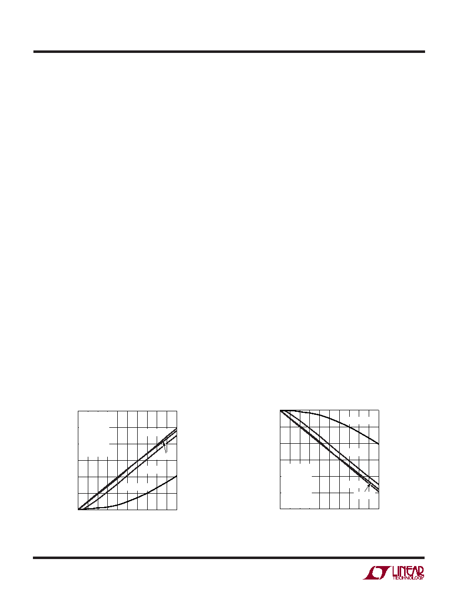
Larger values of input capacitors (CIN > 0.01F) may be
required in certain configurations for antialiasing or gen-
eral input signal filtering. Such capacitors will average the
input sampling charge and the external source resistance
will see a quasi constant input differential impedance. For
the LTC2411, when FO = LOW (internal oscillator and 60Hz
notch), the typical differential input resistance is 5.4M
which will generate a gain error of approximately 0.093ppm
for each ohm of source resistance driving IN+ or IN–.
When FO = HIGH (internal oscillator and 50Hz notch), the
typical differential input resistance is 6.5M
which will
generate a gain error of approximately 0.077ppm for each
ohm of source resistance driving IN+ or IN–. For the
LTC2411-1, the typical differential input resistance is
6M
which will generate a gain error of approximately
0.084ppm for each ohm of source resistance driving IN+
or IN– (FO = LOW). When FO is driven by an external
oscillator with a frequency fEOSC (external conversion
clock operation), the typical differential input resistance is
0.83 1012/fEOSC and each ohm of source resistance
driving IN+ or IN– will result in 0.59 10–6 fEOSCppm gain
error. The effect of the source resistance on the two input
pins is additive with respect to this gain error. The typical
+FS and –FS errors as a function of the sum of the source
resistance seen by IN+ and IN– for large values of CIN are
shown in Figure 15.
In addition to this gain error, an offset error term may also
appear. The offset error is proportional with the mismatch
between the source impedance driving the two input pins
IN+ and IN– and with the difference between the input and
reference common mode voltages. While the input drive
circuit nonzero source impedance combined with the
converter average input current will not degrade the INL
performance, indirect distortion may result from the modu-
lation of the offset error by the common mode component
of the input signal. Thus, when using large CIN capacitor
values, it is advisable to carefully match the source imped-
ance seen by the IN+ and IN– pins. For the LTC2411, when
FO = LOW (internal oscillator and 60Hz notch), every 1
mismatch in source impedance transforms a full-scale
common mode input signal into a differential mode input
signal of 0.093ppm. When FO = HIGH (internal oscillator
and 50Hz notch), every 1
mismatch in source imped-
ance transforms a full-scale common mode input signal
into a differential mode input signal of 0.077ppm. For the
LTC2411-1, when internal oscillator is used (FO = LOW),
every 1
mismatch in source impedance transforms a
full-scale common mode input signal into a differential
mode input signal of 0.084ppm. When FO is driven by an
external oscillator with a frequency fEOSC, every 1 mis-
match in source impedance transforms a full-scale com-
mon mode input signal into a differential mode input
signal of 0.59 10–6 fEOSCppm. Figure 16 shows the
typical offset error due to input common mode voltage for
various values of source resistance imbalance between
the IN+ and IN– pins when large CIN values are used.
If possible, it is desirable to operate with the input signal
common mode voltage very close to the reference signal
common mode voltage as is the case in the ratiometric
measurement of a symmetric bridge. This configuration
APPLICATIO S I FOR ATIO
WU
UU
RSOURCE ()
0 100 200 300 400 500 600 700 800 900 1000
+FS
ERROR
(ppm
OF
V
REF
)
2411 F15a
120
100
80
60
40
20
0
VCC = 5V
REF+ = 5V
REF – = GND
IN+ = 3.75V
IN– = 1.25V
FO = GND
TA = 25°C
CIN = 1F
CIN = 0.1F
CIN = 0.01F
CIN = 10F
Figure 15a. + FS Error vs RSOURCE at IN+ or IN– (Large CIN)
Figure 15b. – FS Error vs RSOURCE at IN
+ or IN– (Large CIN)
RSOURCE ()
0 100 200 300 400 500 600 700 800 900 1000
–
FS
ERROR
(ppm
OF
V
REF
)
2411 F15b
–120
–100
–80
–60
–40
–20
0
VCC = 5V
REF+ = 5V
REF – = GND
IN+ = 1.25V
IN– = 3.75V
FO = GND
TA = 25°C
CIN = 1F
CIN = 0.1F
CIN = 0.01F
CIN = 10F
相关PDF资料 |
PDF描述 |
|---|---|
| LTC2411CMS | IC A/D CONV 24BIT MICRPWR 10MSOP |
| LTC2413CGN | IC A/D CONV 24BIT MICRPWR 16SSOP |
| MS27508E12A22S | CONN RCPT 22POS BOX MNT W/SCKT |
| LTC2410CGN | IC ADC 24BIT DIFF INP/REF 16SSOP |
| LTC1594CS#TRPBF | IC A/D CONV 12BIT SRL 4CH 16SOIC |
相关代理商/技术参数 |
参数描述 |
|---|---|
| LTC2411IMS | 功能描述:IC A/D CONV 24BIT MICRPWR 10MSOP RoHS:否 类别:集成电路 (IC) >> 数据采集 - 模数转换器 系列:- 标准包装:1,000 系列:- 位数:16 采样率(每秒):45k 数据接口:串行 转换器数目:2 功率耗散(最大):315mW 电压电源:模拟和数字 工作温度:0°C ~ 70°C 安装类型:表面贴装 封装/外壳:28-SOIC(0.295",7.50mm 宽) 供应商设备封装:28-SOIC W 包装:带卷 (TR) 输入数目和类型:2 个单端,单极 |
| LTC2411IMS#PBF | 功能描述:IC A/D CONV 24BIT MICRPWR 10MSOP RoHS:是 类别:集成电路 (IC) >> 数据采集 - 模数转换器 系列:- 标准包装:1 系列:microPOWER™ 位数:8 采样率(每秒):1M 数据接口:串行,SPI? 转换器数目:1 功率耗散(最大):- 电压电源:模拟和数字 工作温度:-40°C ~ 125°C 安装类型:表面贴装 封装/外壳:24-VFQFN 裸露焊盘 供应商设备封装:24-VQFN 裸露焊盘(4x4) 包装:Digi-Reel® 输入数目和类型:8 个单端,单极 产品目录页面:892 (CN2011-ZH PDF) 其它名称:296-25851-6 |
| LTC2411IMS#TR | 功能描述:IC A/D CONV 24BIT MICRPWR 10MSOP RoHS:否 类别:集成电路 (IC) >> 数据采集 - 模数转换器 系列:- 标准包装:1,000 系列:- 位数:16 采样率(每秒):45k 数据接口:串行 转换器数目:2 功率耗散(最大):315mW 电压电源:模拟和数字 工作温度:0°C ~ 70°C 安装类型:表面贴装 封装/外壳:28-SOIC(0.295",7.50mm 宽) 供应商设备封装:28-SOIC W 包装:带卷 (TR) 输入数目和类型:2 个单端,单极 |
| LTC2411IMS#TRPBF | 功能描述:IC A/D CONV 24BIT MICRPWR 10MSOP RoHS:是 类别:集成电路 (IC) >> 数据采集 - 模数转换器 系列:- 标准包装:1,000 系列:- 位数:16 采样率(每秒):45k 数据接口:串行 转换器数目:2 功率耗散(最大):315mW 电压电源:模拟和数字 工作温度:0°C ~ 70°C 安装类型:表面贴装 封装/外壳:28-SOIC(0.295",7.50mm 宽) 供应商设备封装:28-SOIC W 包装:带卷 (TR) 输入数目和类型:2 个单端,单极 |
| LTC2412CGN | 功能描述:IC ADC 2CH DIFF-IN 24BIT 16SSOP RoHS:否 类别:集成电路 (IC) >> 数据采集 - 模数转换器 系列:- 标准包装:1,000 系列:- 位数:16 采样率(每秒):45k 数据接口:串行 转换器数目:2 功率耗散(最大):315mW 电压电源:模拟和数字 工作温度:0°C ~ 70°C 安装类型:表面贴装 封装/外壳:28-SOIC(0.295",7.50mm 宽) 供应商设备封装:28-SOIC W 包装:带卷 (TR) 输入数目和类型:2 个单端,单极 |
发布紧急采购,3分钟左右您将得到回复。