- 您现在的位置:买卖IC网 > PDF目录10674 > LTC2413IGN#PBF (Linear Technology)IC A/D CONV 24BIT MICRPWR 16SSOP PDF资料下载
参数资料
| 型号: | LTC2413IGN#PBF |
| 厂商: | Linear Technology |
| 文件页数: | 2/44页 |
| 文件大小: | 0K |
| 描述: | IC A/D CONV 24BIT MICRPWR 16SSOP |
| 标准包装: | 100 |
| 位数: | 24 |
| 采样率(每秒): | 6.8 |
| 数据接口: | MICROWIRE?,串行,SPI? |
| 转换器数目: | 2 |
| 功率耗散(最大): | 1mW |
| 电压电源: | 单电源 |
| 工作温度: | -40°C ~ 85°C |
| 安装类型: | 表面贴装 |
| 封装/外壳: | 16-SSOP(0.154",3.90mm 宽) |
| 供应商设备封装: | 16-SSOP |
| 包装: | 管件 |
| 输入数目和类型: | 1 个差分,双极 |
| 产品目录页面: | 1347 (CN2011-ZH PDF) |
第1页当前第2页第3页第4页第5页第6页第7页第8页第9页第10页第11页第12页第13页第14页第15页第16页第17页第18页第19页第20页第21页第22页第23页第24页第25页第26页第27页第28页第29页第30页第31页第32页第33页第34页第35页第36页第37页第38页第39页第40页第41页第42页第43页第44页
LTC2413
10
sn2413 2413fs
GND (Pins 1, 7, 8, 9, 10, 15, 16): Ground. Multiple ground
pins internally connected for optimum ground current flow
and VCC decoupling. Connect each one of these pins to a
ground plane through a low impedance connection. All seven
pins must be connected to ground for proper operation.
VCC (Pin 2): Positive Supply Voltage. Bypass to GND
(Pin 1) with a 10
F tantalum capacitor in parallel with
0.1
F ceramic capacitor as close to the part as possible.
REF+ (Pin 3), REF– (Pin 4): Differential Reference Input.
The voltage on these pins can have any value between GND
and VCC as long as the reference positive input, REF+, is
maintained more positive than the reference negative
input, REF –, by at least 0.1V.
IN+ (Pin 5), IN– (Pin 6): Differential Analog Input. The voltage
on these pins can have any value between
GND – 0.3V and VCC+0.3V.Withintheselimits, theconverter
bipolar input range (VIN = IN+ – IN–) extends from –0.5
(VREF) to 0.5 (VREF). Outside this input range, the converter
produces unique overrange and underrange output codes.
CS (Pin 11): Active LOW Digital Input. A LOW on this pin
enables the SDO digital output and wakes up the ADC.
Following each conversion, the ADC automatically enters
the Sleep mode and remains in this low power state as
long as CS is HIGH. A LOW-to-HIGH transition on CS
during the Data Output transfer aborts the data transfer
and starts a new conversion.
SDO (Pin 12): Three-State Digital Output. During the Data
Output period, this pin is used as serial data output. When
the chip select CS is HIGH (CS = VCC), the SDO pin is in a
high impedance state. During the Conversion and Sleep
periods, this pin is used as the conversion status output.
The conversion status can be observed by pulling CS LOW.
SCK (Pin 13): Bidirectional Digital Clock Pin. In Internal
Serial Clock Operation mode, SCK is used as digital output
for the internal serial interface clock during the Data
Output period. In External Serial Clock Operation mode,
SCK is used as digital input for the external serial interface
clock during the Data Output period. A weak internal pull-
up is automatically activated in Internal Serial Clock Op-
eration mode. The Serial Clock Operation mode is deter-
mined by the logic level applied to the SCK pin at power up
or during the most recent falling edge of CS.
FO (Pin 14): Frequency Control Pin. Digital input that
controls the ADC’s notch frequencies and conversion
time. When the FO pin is connected to GND (FO = 0V), the
converter uses its internal oscillator and the digital filter
rejects 50Hz and 60Hz simultaneously. When the FO pin is
driven by an external clock signal with a frequency fEOSC,
the converter uses this signal as its system clock and the
digital filter has 87dB minimum rejection in the range
fEOSC/2560 ±14% and 110dB minimum rejection at
fEOSC/2560 ±4%.
PI FU CTIO S
UU
U
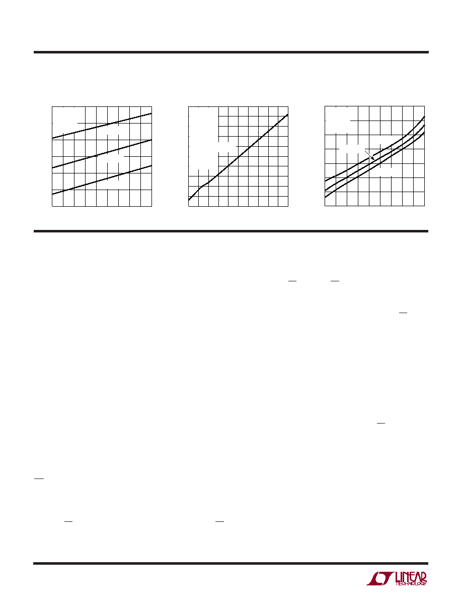
TYPICAL PERFOR A CE CHARACTERISTICS
UW
TEMPERATURE (
°C)
SUPPLY
CURRENT
(
A)
2413 G39
23
22
21
20
19
18
17
16
–45 –30 –15
0
15
30
45
60
75
90
FO = GND
CS = VCC
SCK = NC
SDO = NC
VCC = 5.5V
VCC = 2.7V
VCC = 4.1V
Sleep Current vs Temperature (TA)
OUTPUT DATA RATE (READINGS/SEC)
SUPPLY
CURRENT
(
A)
2413 G38
1100
1000
900
800
700
600
500
400
300
200
100
010 20 30 40 50 60 70 80 90 100
VCC = 5V
REF + = 5V
REF – = GND
IN+ = GND
IN– = GND
TA = 25°C
FO = EXTERNAL OSC
CS = GND
SCK = NC
SDO = NC
TEMPERATURE (
°C)
SUPPLY
CURRENT
(
A)
2413 G37
220
210
200
190
180
170
160
–45 –30 –15
0
15
30
45
60
75
90
FO = GND
CS = GND
SCK = NC
SDO = NC
VCC = 5.5V
VCC = 4.1V
VCC = 2.7V
Conversion Current vs
Output Data Rate
Conversion Current vs
Temperature (TA)
相关PDF资料 |
PDF描述 |
|---|---|
| LTC2411IMS#PBF | IC A/D CONV 24BIT MICRPWR 10MSOP |
| LM2901VNG | IC COMP QUAD SGL SUPPLY 14DIP |
| ISL4245EIRZ | IC 3DRVR/5RCVR RS232 3V 32-QFN |
| NCV2901DR2G | IC COMP QUAD SGL SUPPLY 14SOIC |
| LMV339DTBR2G | IC COMPARATOR GP LV QUAD 14TSSOP |
相关代理商/技术参数 |
参数描述 |
|---|---|
| LTC2414CGN | 功能描述:IC ADC 8CH 24BIT DIFFINPUT28SSOP RoHS:否 类别:集成电路 (IC) >> 数据采集 - 模数转换器 系列:- 标准包装:1,000 系列:- 位数:16 采样率(每秒):45k 数据接口:串行 转换器数目:2 功率耗散(最大):315mW 电压电源:模拟和数字 工作温度:0°C ~ 70°C 安装类型:表面贴装 封装/外壳:28-SOIC(0.295",7.50mm 宽) 供应商设备封装:28-SOIC W 包装:带卷 (TR) 输入数目和类型:2 个单端,单极 |
| LTC2414CGN#PBF | 功能描述:IC ADC 8CH 24BIT DIFFINPUT28SSOP RoHS:是 类别:集成电路 (IC) >> 数据采集 - 模数转换器 系列:- 标准包装:1 系列:microPOWER™ 位数:8 采样率(每秒):1M 数据接口:串行,SPI? 转换器数目:1 功率耗散(最大):- 电压电源:模拟和数字 工作温度:-40°C ~ 125°C 安装类型:表面贴装 封装/外壳:24-VFQFN 裸露焊盘 供应商设备封装:24-VQFN 裸露焊盘(4x4) 包装:Digi-Reel® 输入数目和类型:8 个单端,单极 产品目录页面:892 (CN2011-ZH PDF) 其它名称:296-25851-6 |
| LTC2414CGN#PBF | 制造商:Linear Technology 功能描述:IC ADC 24BIT SSOP-28 |
| LTC2414CGN#TR | 功能描述:IC ADC 8CH 24BIT DIFFINPUT28SSOP RoHS:否 类别:集成电路 (IC) >> 数据采集 - 模数转换器 系列:- 标准包装:1,000 系列:- 位数:16 采样率(每秒):45k 数据接口:串行 转换器数目:2 功率耗散(最大):315mW 电压电源:模拟和数字 工作温度:0°C ~ 70°C 安装类型:表面贴装 封装/外壳:28-SOIC(0.295",7.50mm 宽) 供应商设备封装:28-SOIC W 包装:带卷 (TR) 输入数目和类型:2 个单端,单极 |
| LTC2414CGN#TRPBF | 功能描述:IC ADC 8CH 24BIT DIFFINPUT28SSOP RoHS:是 类别:集成电路 (IC) >> 数据采集 - 模数转换器 系列:- 标准包装:1,000 系列:- 位数:16 采样率(每秒):45k 数据接口:串行 转换器数目:2 功率耗散(最大):315mW 电压电源:模拟和数字 工作温度:0°C ~ 70°C 安装类型:表面贴装 封装/外壳:28-SOIC(0.295",7.50mm 宽) 供应商设备封装:28-SOIC W 包装:带卷 (TR) 输入数目和类型:2 个单端,单极 |
发布紧急采购,3分钟左右您将得到回复。