- 您现在的位置:买卖IC网 > PDF目录10328 > LTC2431CMS (Linear Technology)IC ADC 20BIT DIFFINPUT/REF10MSOP PDF资料下载
参数资料
| 型号: | LTC2431CMS |
| 厂商: | Linear Technology |
| 文件页数: | 3/40页 |
| 文件大小: | 0K |
| 描述: | IC ADC 20BIT DIFFINPUT/REF10MSOP |
| 标准包装: | 50 |
| 位数: | 20 |
| 采样率(每秒): | 7.5 |
| 数据接口: | MICROWIRE?,串行,SPI? |
| 转换器数目: | 2 |
| 功率耗散(最大): | 1mW |
| 电压电源: | 单电源 |
| 工作温度: | 0°C ~ 70°C |
| 安装类型: | 表面贴装 |
| 封装/外壳: | 10-TFSOP,10-MSOP(0.118",3.00mm 宽) |
| 供应商设备封装: | 10-MSOP |
| 包装: | 管件 |
| 输入数目和类型: | 1 个差分,双极 |
| 配用: | DC586A-ND - BOARD DELTA SIGMA ADC LTC2431 |
第1页第2页当前第3页第4页第5页第6页第7页第8页第9页第10页第11页第12页第13页第14页第15页第16页第17页第18页第19页第20页第21页第22页第23页第24页第25页第26页第27页第28页第29页第30页第31页第32页第33页第34页第35页第36页第37页第38页第39页第40页
LTC2430/LTC2431
11
24301f
CONVERTER OPERATION
Converter Operation Cycle
The LTC2430/LTC2431 are low power, delta-sigma analog-
to-digital converters with an easy-to-use 3-wire serial inter-
face(seeFigure1).Their operationismadeupofthreestates.
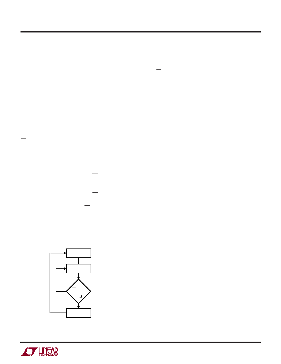
The converters’ operating cycle begins with the conversion,
followed by the low power sleep state and ends with the data
output (see Figure 2). The 3-wire interface consists of serial
data output (SDO), serial clock (SCK) and chip select (CS).
Initially, the LTC2430/LTC2431 perform a conversion.
Once the conversion is complete, the device enters the
sleep state. The part remains in the sleep state as long as
CS is HIGH. While in this sleep state, power consumption
is reduced by nearly two orders of magnitude. The conver-
sion result is held indefinitely in a static shift register while
the converter is in the sleep state.
Once CS is pulled LOW, the device exits the low power mode
and enters the data output state. If CS is pulled HIGH be-
fore the first rising edge of SCK, the device returns to the
low power sleep mode and the conversion result is still held
in the internal static shift register. If CS remains LOW after
the first rising edge of SCK, the device begins outputting
the conversion result. Taking CS high at this point will
terminate the data output state and start a new conversion.
There is no latency in the conversion result. The data out-
put corresponds to the conversion just performed. This
result is shifted out on the serial data out pin (SDO) under
the control of the serial clock (SCK). Data is updated on the
falling edge of SCK allowing the user to reliably latch data
on the rising edge of SCK (see Figure 3). The data output
state is concluded once 24 bits are read out of the ADC or
when CS is brought HIGH. The device automatically initiates
a new conversion and the cycle repeats.
Through timing control of the CS and SCK pins, the
LTC2430/LTC2431 offer several flexible modes of
operation (internal or external SCK and free-running
conversion modes). These various modes do not require
programming configuration registers; moreover, they do
not disturb the cyclic operation described above. These
modes of operation are described in detail in the Serial
Interface Timing Modes section.
Conversion Clock
A major advantage the delta-sigma converter offers over
conventional type converters is an on-chip digital filter
(commonly implemented as a Sinc or Comb filter). For
high resolution, low frequency applications, this filter is
typically designed to reject line frequencies of 50Hz or
60Hz plus their harmonics. The filter rejection perfor-
mance is directly related to the accuracy of the converter
system clock. The LTC2430/LTC2431 incorporate a highly
accurate on-chip oscillator. This eliminates the need for
external frequency setting components such as crystals or
oscillators. Clocked by the on-chip oscillator, the LTC2430/
LTC2431 achieve a minimum of 110dB rejection at the line
frequency (50Hz or 60Hz
±2%).
Ease of Use
The LTC2430/LTC2431 data output has no latency, filter
settling delay or redundant data associated with the
conversion cycle. There is a one-to-one correspondence
between the conversion and the output data. Therefore,
multiplexing multiple analog inputs is easy.
The LTC2430/LTC2431 perform offset and full-scale cali-
brations in every conversion cycle. This calibration is trans-
parent to the user and has no effect on the cyclic operation
described above. The advantage of continuous calibration
is extreme stability of offset and full-scale readings with
respect to time, supply voltage change and temperature
drift.
Figure 2. LTC2430/LTC2431 State Transition Diagram
CONVERT
SLEEP
DATA OUTPUT
2431 F02
TRUE
FALSE
CS = LOW
AND
SCK
APPLICATIO S I FOR ATIO
WU
UU
相关PDF资料 |
PDF描述 |
|---|---|
| VI-B3V-IW-B1 | CONVERTER MOD DC/DC 5.8V 100W |
| VI-B3T-IX-B1 | CONVERTER MOD DC/DC 6.5V 75W |
| CS5512-BSZR | IC ADC 20BIT EXTERNAL OSC 8-SOIC |
| VI-B2X-IX-B1 | CONVERTER MOD DC/DC 5.2V 75W |
| LTC1197LCS8 | IC ADC 10BIT 250KHZ W/SD 8-SOIC |
相关代理商/技术参数 |
参数描述 |
|---|---|
| LTC2431CMS#PBF | 功能描述:IC ADC 20BIT DIFFINPUT/REF10MSOP RoHS:是 类别:集成电路 (IC) >> 数据采集 - 模数转换器 系列:- 标准包装:1 系列:microPOWER™ 位数:8 采样率(每秒):1M 数据接口:串行,SPI? 转换器数目:1 功率耗散(最大):- 电压电源:模拟和数字 工作温度:-40°C ~ 125°C 安装类型:表面贴装 封装/外壳:24-VFQFN 裸露焊盘 供应商设备封装:24-VQFN 裸露焊盘(4x4) 包装:Digi-Reel® 输入数目和类型:8 个单端,单极 产品目录页面:892 (CN2011-ZH PDF) 其它名称:296-25851-6 |
| LTC2431CMS#TR | 功能描述:IC ADC 20BIT DIFFINPUT/REF10MSOP RoHS:否 类别:集成电路 (IC) >> 数据采集 - 模数转换器 系列:- 标准包装:2,500 系列:- 位数:16 采样率(每秒):15 数据接口:MICROWIRE?,串行,SPI? 转换器数目:1 功率耗散(最大):480µW 电压电源:单电源 工作温度:-40°C ~ 85°C 安装类型:表面贴装 封装/外壳:38-WFQFN 裸露焊盘 供应商设备封装:38-QFN(5x7) 包装:带卷 (TR) 输入数目和类型:16 个单端,双极;8 个差分,双极 配用:DC1011A-C-ND - BOARD DELTA SIGMA ADC LTC2494 |
| LTC2431CMS#TRPBF | 功能描述:IC ADC 20BIT DIFFINPUT/REF10MSOP RoHS:是 类别:集成电路 (IC) >> 数据采集 - 模数转换器 系列:- 标准包装:2,500 系列:- 位数:16 采样率(每秒):15 数据接口:MICROWIRE?,串行,SPI? 转换器数目:1 功率耗散(最大):480µW 电压电源:单电源 工作温度:-40°C ~ 85°C 安装类型:表面贴装 封装/外壳:38-WFQFN 裸露焊盘 供应商设备封装:38-QFN(5x7) 包装:带卷 (TR) 输入数目和类型:16 个单端,双极;8 个差分,双极 配用:DC1011A-C-ND - BOARD DELTA SIGMA ADC LTC2494 |
| LTC2431IMS | 功能描述:IC ADC 20BIT DIFFINPUT/REF10MSOP RoHS:否 类别:集成电路 (IC) >> 数据采集 - 模数转换器 系列:- 标准包装:1,000 系列:- 位数:16 采样率(每秒):45k 数据接口:串行 转换器数目:2 功率耗散(最大):315mW 电压电源:模拟和数字 工作温度:0°C ~ 70°C 安装类型:表面贴装 封装/外壳:28-SOIC(0.295",7.50mm 宽) 供应商设备封装:28-SOIC W 包装:带卷 (TR) 输入数目和类型:2 个单端,单极 |
| LTC2431IMS#PBF | 功能描述:IC ADC 20BIT DIFFINPUT/REF10MSOP RoHS:是 类别:集成电路 (IC) >> 数据采集 - 模数转换器 系列:- 标准包装:1,000 系列:- 位数:16 采样率(每秒):45k 数据接口:串行 转换器数目:2 功率耗散(最大):315mW 电压电源:模拟和数字 工作温度:0°C ~ 70°C 安装类型:表面贴装 封装/外壳:28-SOIC(0.295",7.50mm 宽) 供应商设备封装:28-SOIC W 包装:带卷 (TR) 输入数目和类型:2 个单端,单极 |
发布紧急采购,3分钟左右您将得到回复。