- 您现在的位置:买卖IC网 > PDF目录2006 > LTC2431IMS#TRPBF (Linear Technology)IC ADC 20BIT DIFFINPUT/REF10MSOP PDF资料下载
参数资料
| 型号: | LTC2431IMS#TRPBF |
| 厂商: | Linear Technology |
| 文件页数: | 2/40页 |
| 文件大小: | 0K |
| 描述: | IC ADC 20BIT DIFFINPUT/REF10MSOP |
| 标准包装: | 2,500 |
| 位数: | 20 |
| 采样率(每秒): | 7.5 |
| 数据接口: | MICROWIRE?,串行,SPI? |
| 转换器数目: | 2 |
| 功率耗散(最大): | 1mW |
| 电压电源: | 单电源 |
| 工作温度: | -40°C ~ 85°C |
| 安装类型: | 表面贴装 |
| 封装/外壳: | 10-TFSOP,10-MSOP(0.118",3.00mm 宽) |
| 供应商设备封装: | 10-MSOP |
| 包装: | 带卷 (TR) |
| 输入数目和类型: | 1 个差分,双极 |
| 配用: | DC586A-ND - BOARD DELTA SIGMA ADC LTC2431 |
第1页当前第2页第3页第4页第5页第6页第7页第8页第9页第10页第11页第12页第13页第14页第15页第16页第17页第18页第19页第20页第21页第22页第23页第24页第25页第26页第27页第28页第29页第30页第31页第32页第33页第34页第35页第36页第37页第38页第39页第40页
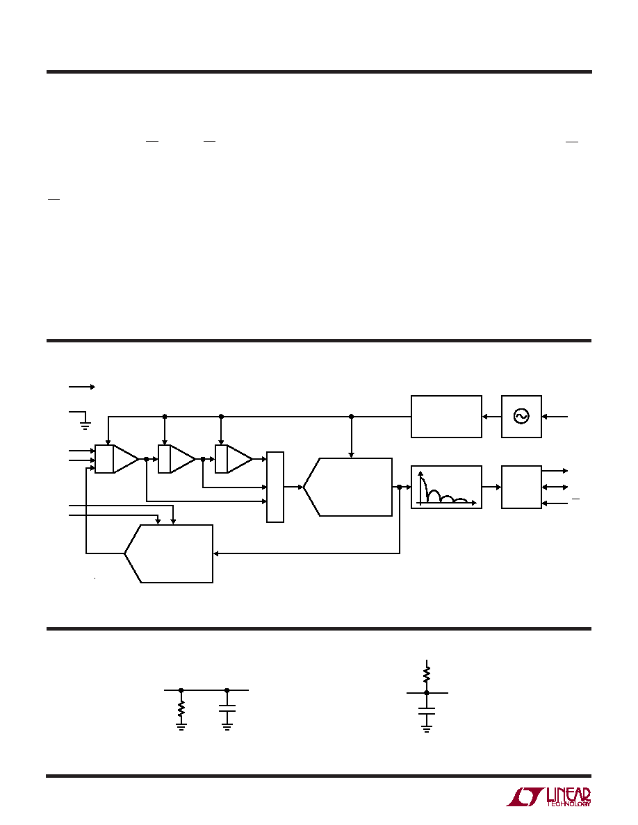
LTC2430/LTC2431
10
24301f
Figure 1
UU
W
FU CTIO AL BLOCK DIAGRA
AUTOCALIBRATION
AND CONTROL
DAC
DECIMATING FIR
INTERNAL
OSCILLATOR
SERIAL
INTERFACE
ADC
∑
∫
GND
VCC
IN+
IN–
SDO
SCK
REF+
REF –
CS
FO
(INT/EXT)
2431 FD
+
–
TEST CIRCUITS
1.69k
SDO
2431 TA03
Hi-Z TO VOH
VOL TO VOH
VOH TO Hi-Z
CLOAD = 20pF
1.69k
SDO
2431 TA04
Hi-Z TO VOL
VOH TO VOL
VOL TO Hi-Z
CLOAD = 20pF
VCC
SDO (Pin 8): Three-State Digital Output. During the Data
Output period, this pin is used as the serial data output.
When the chip select CS is HIGH (CS = VCC), the SDO pin
is in a high impedance state. During the Conversion and
Sleep periods, this pin is used as the conversion status
output. The conversion status can be observed by pulling
CS LOW.
SCK (Pin 9): Bidirectional Digital Clock Pin. In Internal
Serial Clock Operation mode, SCK is used as the digital
output for the internal serial interface clock during the Data
Output period. In External Serial Clock Operation mode,
SCK is used as the digital input for the external serial
interface clock during the Data Output period. A weak
internal pull-up is automatically activated in Internal Serial
Clock Operation mode. The Serial Clock Operation mode is
determined by the logic level applied to the SCK pin at
power up or during the most recent falling edge of CS.
FO (Pin 10): Frequency Control Pin. Digital input that
controls the ADC’s notch frequencies and conversion
time. When the FO pin is connected to VCC (FO = VCC), the
converter uses its internal oscillator and the digital filter
first null is located at 50Hz. When the FO pin is connected
to GND (FO = OV), the converter uses its internal oscillator
and the digital filter first null is located at 60Hz. When FO
is driven by an external clock signal with a frequency fEOSC,
the converter uses this signal as its system clock and the
digital filter first null is located at a frequency fEOSC/2560.
UU
U
PI FU CTIO S (LTC2431)
相关PDF资料 |
PDF描述 |
|---|---|
| LTC2433-1IMS#TRPBF | IC ADC DIFF 16BIT 3WIRE 10-MSOP |
| LTC2435CGN#TRPBF | IC ADC DIFF I/REF 20BIT 16-SSOP |
| LTC2442IG#PBF | IC ADC 24BIT 4CH 36-SSOP |
| LTC2446IUHF#TRPBF | IC ADC 24BIT 8CH HI SPEED 38QFN |
| LTC2448IUHF#TRPBF | IC ADC 24BIT HI SPEED 38QFN |
相关代理商/技术参数 |
参数描述 |
|---|---|
| LTC2433-1CMS | 功能描述:IC ADC DIFF 16BIT 3WIRE 10-MSOP RoHS:否 类别:集成电路 (IC) >> 数据采集 - 模数转换器 系列:- 标准包装:2,500 系列:- 位数:16 采样率(每秒):15 数据接口:MICROWIRE?,串行,SPI? 转换器数目:1 功率耗散(最大):480µW 电压电源:单电源 工作温度:-40°C ~ 85°C 安装类型:表面贴装 封装/外壳:38-WFQFN 裸露焊盘 供应商设备封装:38-QFN(5x7) 包装:带卷 (TR) 输入数目和类型:16 个单端,双极;8 个差分,双极 配用:DC1011A-C-ND - BOARD DELTA SIGMA ADC LTC2494 |
| LTC2433-1CMS#PBF | 功能描述:IC ADC DIFF 16BIT 3WIRE 10-MSOP RoHS:是 类别:集成电路 (IC) >> 数据采集 - 模数转换器 系列:- 标准包装:1 系列:microPOWER™ 位数:8 采样率(每秒):1M 数据接口:串行,SPI? 转换器数目:1 功率耗散(最大):- 电压电源:模拟和数字 工作温度:-40°C ~ 125°C 安装类型:表面贴装 封装/外壳:24-VFQFN 裸露焊盘 供应商设备封装:24-VQFN 裸露焊盘(4x4) 包装:Digi-Reel® 输入数目和类型:8 个单端,单极 产品目录页面:892 (CN2011-ZH PDF) 其它名称:296-25851-6 |
| LTC2433-1CMS#TR | 功能描述:IC CONV A/D 16BIT DIFF 10-MSOP RoHS:否 类别:集成电路 (IC) >> 数据采集 - 模数转换器 系列:- 标准包装:2,500 系列:- 位数:16 采样率(每秒):15 数据接口:MICROWIRE?,串行,SPI? 转换器数目:1 功率耗散(最大):480µW 电压电源:单电源 工作温度:-40°C ~ 85°C 安装类型:表面贴装 封装/外壳:38-WFQFN 裸露焊盘 供应商设备封装:38-QFN(5x7) 包装:带卷 (TR) 输入数目和类型:16 个单端,双极;8 个差分,双极 配用:DC1011A-C-ND - BOARD DELTA SIGMA ADC LTC2494 |
| LTC2433-1CMS#TRPBF | 功能描述:IC ADC DIFF 16BIT 3WIRE 10-MSOP RoHS:是 类别:集成电路 (IC) >> 数据采集 - 模数转换器 系列:- 标准包装:2,500 系列:- 位数:16 采样率(每秒):15 数据接口:MICROWIRE?,串行,SPI? 转换器数目:1 功率耗散(最大):480µW 电压电源:单电源 工作温度:-40°C ~ 85°C 安装类型:表面贴装 封装/外壳:38-WFQFN 裸露焊盘 供应商设备封装:38-QFN(5x7) 包装:带卷 (TR) 输入数目和类型:16 个单端,双极;8 个差分,双极 配用:DC1011A-C-ND - BOARD DELTA SIGMA ADC LTC2494 |
| LTC2433-1CMSPBF | 制造商:Linear Technology 功能描述:ADC,LTC2433 16bit diff D-S SPI MSOP |
发布紧急采购,3分钟左右您将得到回复。