- 您现在的位置:买卖IC网 > PDF目录10330 > LTC2435CGN (Linear Technology)IC ADC DIFF I/REF 20BIT 16-SSOP PDF资料下载
参数资料
| 型号: | LTC2435CGN |
| 厂商: | Linear Technology |
| 文件页数: | 4/42页 |
| 文件大小: | 0K |
| 描述: | IC ADC DIFF I/REF 20BIT 16-SSOP |
| 标准包装: | 100 |
| 位数: | 20 |
| 采样率(每秒): | 15 |
| 数据接口: | MICROWIRE?,串行,SPI? |
| 转换器数目: | 2 |
| 功率耗散(最大): | 1mW |
| 电压电源: | 单电源 |
| 工作温度: | 0°C ~ 70°C |
| 安装类型: | 表面贴装 |
| 封装/外壳: | 16-SSOP(0.154",3.90mm 宽) |
| 供应商设备封装: | 16-SSOP |
| 包装: | 管件 |
| 输入数目和类型: | 1 个差分,双极 |
第1页第2页第3页当前第4页第5页第6页第7页第8页第9页第10页第11页第12页第13页第14页第15页第16页第17页第18页第19页第20页第21页第22页第23页第24页第25页第26页第27页第28页第29页第30页第31页第32页第33页第34页第35页第36页第37页第38页第39页第40页第41页第42页
LTC2435/LTC2435-1
12
24351fc
For more information www.linear.com/LTC2435
CONVERTER OPERATION
Converter Operation Cycle
The LTC2435/LTC2435-1 are low power, delta-sigma
analog-to-digital converters with an easy to use 3-wire
serial interface (see Figure 1). Their operation is made
up of three states. The converter operating cycle begins
with the conversion, followed by the sleep state and ends
with the data output (see Figure 2). The 3-wire interface
consists of serial data output (SDO), serial clock (SCK)
and chip select (CS).
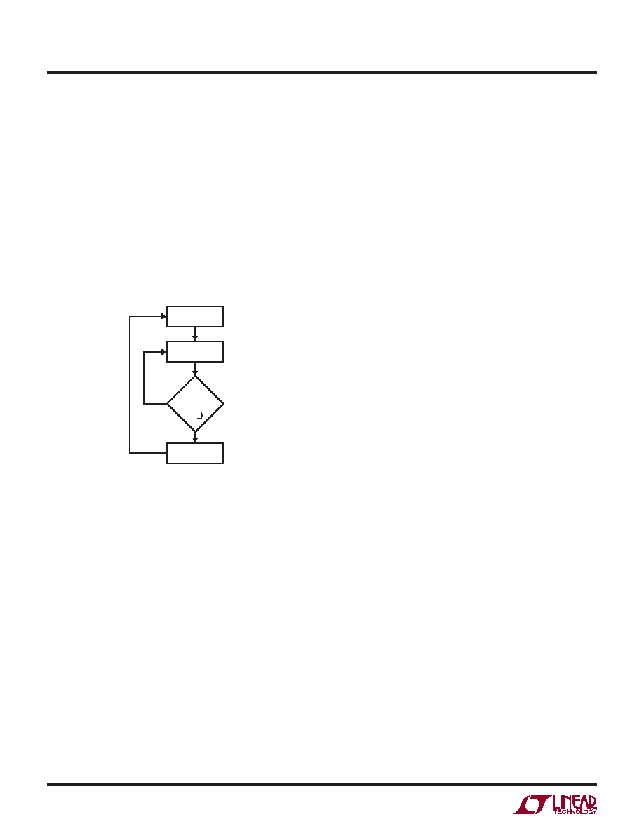
Figure 2. LTC2435 State Transition Diagram
Initially, the LTC2435/LTC2435-1 perform a conversion.
Once the conversion is complete, the device enters the
sleep state. While in this sleep state, power consumption
is reduced by an order of magnitude if CS is HIGH. The
part remains in the sleep state as long as CS is HIGH.
The conversion result is held indefinitely in a static shift
register while the converter is in the sleep state.
Once CS is pulled LOW, the device exits the low power
sleep mode and enters the data output state. If CS is pulled
HIGH before the first rising edge of SCK, the device returns
to the sleep mode and the conversion result is still held in
the internal static shift register. If CS remains LOW after
the first rising edge of SCK, the device begins outputting
the conversion result. Taking CS HIGH at this point will
terminate the data output state and start a new conversion.
applicaTions inForMaTion
Thereisnolatencyintheconversionresult.Thedataoutput
corresponds to the conversion just performed. This result
is shifted out on the serial data out pin (SDO) under the
control of the serial clock (SCK). Data is updated on the
falling edge of SCK allowing the user to reliably latch data
on the rising edge of SCK (see Figure 3). The data output
state is concluded once 24 bits are read out of the ADC
or when CS is brought HIGH. The device automatically
initiates a new conversion and the cycle repeats.
Through timing control of the CS and SCK pins, the
LTC2435/LTC2435-1 offer several flexible modes of
operation (internal or external SCK and free-running
conversion modes). These various modes do not require
programming configuration registers; moreover, they do
not disturb the cyclic operation described above. These
modes of operation are described in detail in the Serial
Interface Timing Modes section.
Conversion Clock
A major advantage the delta-sigma converter offers over
conventional type converters is an on-chip digital filter
(commonly implemented as a Sinc or Comb filter). For
high resolution, low frequency applications, this filter is
typicallydesignedtorejectlinefrequenciesof50Hzor60Hz
plus their harmonics. The filter rejection performance is
directly related to the accuracy of the converter system
clock. The LTC2435/LTC2435-1 incorporate a highly
accurate on-chip oscillator. This eliminates the need for
external frequency setting components such as crystals
or oscillators. Clocked by the on-chip oscillator, the
LTC2435 achieves a minimum of 110dB rejection at the
line frequency (50Hz or 60Hz ±2%), while the LTC2435-1
achieves a minimum of 87db rejection at 50Hz ±2% and
60Hz ±2% simultaneously.
Ease of Use
The LTC2435/LTC2435-1 data output has no latency,
filter settling delay or redundant data associated with the
conversion cycle. There is a one-to-one correspondence
between the conversion and the output data. Therefore,
multiplexing multiple analog voltages is easy.
CONVERT
SLEEP
DATA OUTPUT
2435 F02
TRUE
FALSE
CS = LOW
AND
SCK
相关PDF资料 |
PDF描述 |
|---|---|
| MS27473E14F15S | CONN PLUG 15POS STRAIGHT W/SCKT |
| D38999/24WA98AN | CONN HSG RCPT 3POS JAM NUT PINS |
| D38999/20JF11PALC | CONN HSG RCPT 11POS WALL MT PINS |
| MS27508E20A16P | CONN RCPT 16POS BOX MNT W/PINS |
| D38999/20JG41PNLC | CONN HSG RCPT 41POS WALL MT PINS |
相关代理商/技术参数 |
参数描述 |
|---|---|
| LTC2435CGN#PBF | 功能描述:IC ADC DIFF I/REF 20BIT 16-SSOP RoHS:是 类别:集成电路 (IC) >> 数据采集 - 模数转换器 系列:- 标准包装:2,500 系列:- 位数:16 采样率(每秒):15 数据接口:MICROWIRE?,串行,SPI? 转换器数目:1 功率耗散(最大):480µW 电压电源:单电源 工作温度:-40°C ~ 85°C 安装类型:表面贴装 封装/外壳:38-WFQFN 裸露焊盘 供应商设备封装:38-QFN(5x7) 包装:带卷 (TR) 输入数目和类型:16 个单端,双极;8 个差分,双极 配用:DC1011A-C-ND - BOARD DELTA SIGMA ADC LTC2494 |
| LTC2435CGN#TR | 功能描述:IC CONV A/D 20BIT DIFF 16-SSOP RoHS:否 类别:集成电路 (IC) >> 数据采集 - 模数转换器 系列:- 标准包装:2,500 系列:- 位数:16 采样率(每秒):15 数据接口:MICROWIRE?,串行,SPI? 转换器数目:1 功率耗散(最大):480µW 电压电源:单电源 工作温度:-40°C ~ 85°C 安装类型:表面贴装 封装/外壳:38-WFQFN 裸露焊盘 供应商设备封装:38-QFN(5x7) 包装:带卷 (TR) 输入数目和类型:16 个单端,双极;8 个差分,双极 配用:DC1011A-C-ND - BOARD DELTA SIGMA ADC LTC2494 |
| LTC2435CGN#TRPBF | 功能描述:IC ADC DIFF I/REF 20BIT 16-SSOP RoHS:是 类别:集成电路 (IC) >> 数据采集 - 模数转换器 系列:- 产品培训模块:Lead (SnPb) Finish for COTS Obsolescence Mitigation Program 标准包装:2,500 系列:- 位数:12 采样率(每秒):3M 数据接口:- 转换器数目:- 功率耗散(最大):- 电压电源:- 工作温度:- 安装类型:表面贴装 封装/外壳:SOT-23-6 供应商设备封装:SOT-23-6 包装:带卷 (TR) 输入数目和类型:- |
| LTC2435IGN | 功能描述:IC CONV A/D 20BIT DIFF 16-SSOP RoHS:否 类别:集成电路 (IC) >> 数据采集 - 模数转换器 系列:- 标准包装:2,500 系列:- 位数:16 采样率(每秒):15 数据接口:MICROWIRE?,串行,SPI? 转换器数目:1 功率耗散(最大):480µW 电压电源:单电源 工作温度:-40°C ~ 85°C 安装类型:表面贴装 封装/外壳:38-WFQFN 裸露焊盘 供应商设备封装:38-QFN(5x7) 包装:带卷 (TR) 输入数目和类型:16 个单端,双极;8 个差分,双极 配用:DC1011A-C-ND - BOARD DELTA SIGMA ADC LTC2494 |
| LTC2435IGN#PBF | 功能描述:IC ADC DIFF I/REF 20BIT 16-SSOP RoHS:是 类别:集成电路 (IC) >> 数据采集 - 模数转换器 系列:- 标准包装:2,500 系列:- 位数:16 采样率(每秒):15 数据接口:MICROWIRE?,串行,SPI? 转换器数目:1 功率耗散(最大):480µW 电压电源:单电源 工作温度:-40°C ~ 85°C 安装类型:表面贴装 封装/外壳:38-WFQFN 裸露焊盘 供应商设备封装:38-QFN(5x7) 包装:带卷 (TR) 输入数目和类型:16 个单端,双极;8 个差分,双极 配用:DC1011A-C-ND - BOARD DELTA SIGMA ADC LTC2494 |
发布紧急采购,3分钟左右您将得到回复。