- 您现在的位置:买卖IC网 > PDF目录10296 > LTC2440CGN#TRPBF (Linear Technology)IC ADC DIFFER 24-BIT HS 16-SSOP PDF资料下载
参数资料
| 型号: | LTC2440CGN#TRPBF |
| 厂商: | Linear Technology |
| 文件页数: | 3/28页 |
| 文件大小: | 0K |
| 描述: | IC ADC DIFFER 24-BIT HS 16-SSOP |
| 标准包装: | 2,500 |
| 位数: | 24 |
| 采样率(每秒): | 3.5k |
| 数据接口: | MICROWIRE?,串行,SPI? |
| 转换器数目: | 2 |
| 功率耗散(最大): | 40mW |
| 电压电源: | 单电源 |
| 工作温度: | 0°C ~ 70°C |
| 安装类型: | 表面贴装 |
| 封装/外壳: | 16-SSOP(0.154",3.90mm 宽) |
| 供应商设备封装: | 16-SSOP |
| 包装: | 带卷 (TR) |
| 输入数目和类型: | 1 个差分,双极 |
| 配用: | DC570A-ND - BOARD DELTA SIGMA ADC LTC2440 |
第1页第2页当前第3页第4页第5页第6页第7页第8页第9页第10页第11页第12页第13页第14页第15页第16页第17页第18页第19页第20页第21页第22页第23页第24页第25页第26页第27页第28页
LTC2440
11
2440fd
APPLICATIONS INFORMATION
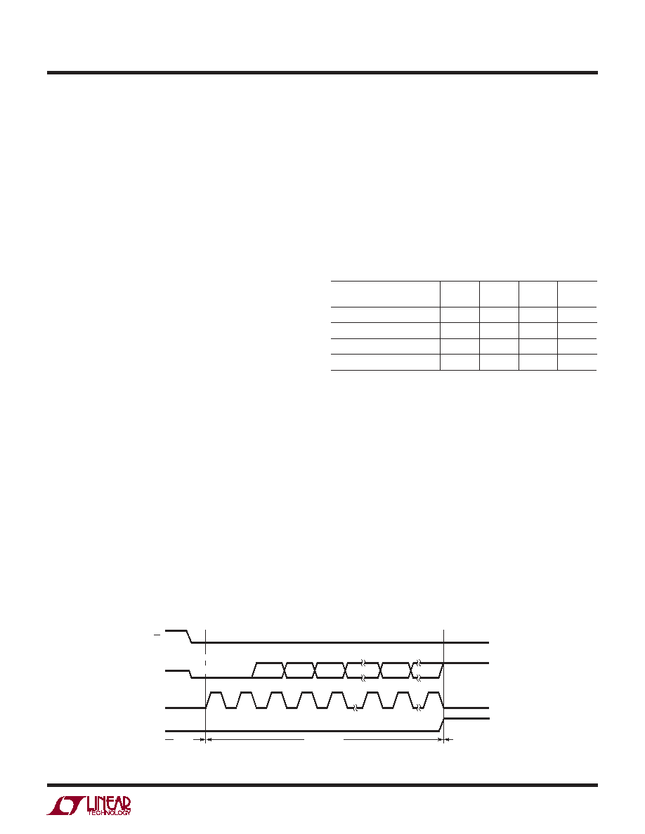
Figure 3. Output Data Timing
0.5 VREF where VREF = REF+ – REF–. Outside this range,
the converter indicates the overrange or the underrange
condition using distinct output codes.
Output Data Format
The LTC2440 serial output data stream is 32-bits long.
The rst 3-bits represent status information indicating
the sign and conversion state. The next 24-bits are the
conversion result, MSB rst. The remaining 5-bits are
sub LSBs beyond the 24-bit level that may be included in
averaging or discarded without loss of resolution. In the
case of ultrahigh resolution modes, more than 24 effec-
tive bits of performance are possible (see Table 3). Under
these conditions, sub LSBs are included in the conversion
result and represent useful information beyond the 24-bit
level. The third and fourth bit together are also used to
indicate an underrange condition (the differential input
voltage is below –FS) or an overrange condition (the dif-
ferential input voltage is above +FS). For input conditions
in excess of twice full scale (|VIN| ≥ VREF), the converter
may indicate either overrange or underrange. Once the
input returns to the normal operating range, the conversion
result is immediately accurate within the specications of
the device.
Bit 31 (rst output bit) is the end of conversion (EOC)
indicator. This bit is available at the SDO pin during the
conversion and sleep states whenever the CS pin is LOW.
This bit is HIGH during the conversion and goes LOW
when the conversion is complete.
Bit 30 (second output bit) is a dummy bit (DMY) and is
always LOW.
Bit 29 (third output bit) is the conversion result sign
indicator (SIG). If VIN is >0, this bit is HIGH. If VIN is <0,
this bit is LOW.
Bit 28 (fourth output bit) is the most signicant bit (MSB) of
the result. This bit in conjunction with Bit 29 also provides
the underrange or overrange indication. If both Bit 29 and
Bit 28 are HIGH, the differential input voltage is above +FS.
If both Bit 29 and Bit 28 are LOW, the differential input
voltage is below –FS.
The function of these bits is summarized in Table 1.
Table 1. LTC2440 Status Bits
Input Range
Bit 31
EOC
Bit 30
DMY
Bit 29
SIG
Bit 28
MSB
VIN ≥ 0.5 VREF
0011
0V ≤ VIN < 0.5 VREF
0010
–0.5 VREF ≤ VIN < 0V
0001
VIN < –0.5 VREF
0000
Bits ranging from 28 to 5 are the 24-bit conversion result
MSB rst.
Bit 5 is the Least Signicant Bit (LSB).
Bits ranging from 4 to 0 are sub LSBs below the 24-bit
level. Bits 4 to bit 0 may be included in averaging or dis-
carded without loss of resolution.
Data is shifted out of the SDO pin under control of the
serial clock (SCK), see Figure 3. Whenever CS is HIGH,
SDO remains high impedance.
In order to shift the conversion result out of the device,
CS must rst be driven LOW. EOC is seen at the SDO pin
of the device once CS is pulled LOW. EOC changes real
time from HIGH to LOW at the completion of a conversion.
This signal may be used as an interrupt for an external
MSB
SIG
“0”
1
2
3
4
5
262732
BIT 0
BIT 27
BIT 5
LSB24
BIT 28
BIT 29
BIT 30
SDO
SCK
BUSY
CS
EOC
BIT 31
SLEEP
DATA OUTPUT
CONVERSION
2440 F03
Hi-Z
相关PDF资料 |
PDF描述 |
|---|---|
| VE-BNB-IW-B1 | CONVERTER MOD DC/DC 95V 100W |
| EN3P10M26SX | CONN RCPT 10POS MALE PANEL #26 |
| D38999/26KA98SNLC | CONN HSG PLUG 3POS STRGHT SCKT |
| LTC2440CGN#TR | IC CONV A/D 24-BIT DIFF 16-SSOP |
| VE-B6P-IX-B1 | CONVERTER MOD DC/DC 13.8V 75W |
相关代理商/技术参数 |
参数描述 |
|---|---|
| LTC2440IGN | 功能描述:IC ADC DIFFER 24-BIT HS 16-SSOP RoHS:否 类别:集成电路 (IC) >> 数据采集 - 模数转换器 系列:- 标准包装:1,000 系列:- 位数:16 采样率(每秒):45k 数据接口:串行 转换器数目:2 功率耗散(最大):315mW 电压电源:模拟和数字 工作温度:0°C ~ 70°C 安装类型:表面贴装 封装/外壳:28-SOIC(0.295",7.50mm 宽) 供应商设备封装:28-SOIC W 包装:带卷 (TR) 输入数目和类型:2 个单端,单极 |
| LTC2440IGN#PBF | 功能描述:IC ADC DIFFER 24-BIT HS 16-SSOP RoHS:是 类别:集成电路 (IC) >> 数据采集 - 模数转换器 系列:- 标准包装:1 系列:microPOWER™ 位数:8 采样率(每秒):1M 数据接口:串行,SPI? 转换器数目:1 功率耗散(最大):- 电压电源:模拟和数字 工作温度:-40°C ~ 125°C 安装类型:表面贴装 封装/外壳:24-VFQFN 裸露焊盘 供应商设备封装:24-VQFN 裸露焊盘(4x4) 包装:Digi-Reel® 输入数目和类型:8 个单端,单极 产品目录页面:892 (CN2011-ZH PDF) 其它名称:296-25851-6 |
| LTC2440IGN#PBF | 制造商:Linear Technology 功能描述:A/D Converter (A-D) IC 制造商:Linear Technology 功能描述:IC, ADC, 24BIT, 3.5KHZ, SSOP-16 |
| LTC2440IGN#TR | 功能描述:IC CONV A/D 24-BIT DIFF 16-SSOP RoHS:否 类别:集成电路 (IC) >> 数据采集 - 模数转换器 系列:- 标准包装:1,000 系列:- 位数:16 采样率(每秒):45k 数据接口:串行 转换器数目:2 功率耗散(最大):315mW 电压电源:模拟和数字 工作温度:0°C ~ 70°C 安装类型:表面贴装 封装/外壳:28-SOIC(0.295",7.50mm 宽) 供应商设备封装:28-SOIC W 包装:带卷 (TR) 输入数目和类型:2 个单端,单极 |
| LTC2440IGN#TRPBF | 功能描述:IC ADC DIFFER 24-BIT HS 16-SSOP RoHS:是 类别:集成电路 (IC) >> 数据采集 - 模数转换器 系列:- 标准包装:1,000 系列:- 位数:16 采样率(每秒):45k 数据接口:串行 转换器数目:2 功率耗散(最大):315mW 电压电源:模拟和数字 工作温度:0°C ~ 70°C 安装类型:表面贴装 封装/外壳:28-SOIC(0.295",7.50mm 宽) 供应商设备封装:28-SOIC W 包装:带卷 (TR) 输入数目和类型:2 个单端,单极 |
发布紧急采购,3分钟左右您将得到回复。