参数资料
| 型号: | LTC2483IDD#TRPBF |
| 厂商: | Linear Technology |
| 文件页数: | 15/34页 |
| 文件大小: | 0K |
| 描述: | IC ADC 16BIT I2C 10-DFN |
| 标准包装: | 2,500 |
| 位数: | 16 |
| 采样率(每秒): | 6.8 |
| 数据接口: | I²C,串行 |
| 转换器数目: | 1 |
| 功率耗散(最大): | 480µW |
| 电压电源: | 单电源 |
| 工作温度: | -40°C ~ 85°C |
| 安装类型: | 表面贴装 |
| 封装/外壳: | 10-WFDFN 裸露焊盘 |
| 供应商设备封装: | 10-DFN(3x3) |
| 包装: | 带卷 (TR) |
| 输入数目和类型: | 1 个差分,双极 |
| 配用: | DC955A-ND - BOARD DELTA SIGMA ADC LTC2483 |
第1页第2页第3页第4页第5页第6页第7页第8页第9页第10页第11页第12页第13页第14页当前第15页第16页第17页第18页第19页第20页第21页第22页第23页第24页第25页第26页第27页第28页第29页第30页第31页第32页第33页第34页
LTC2483
2483fc
Output Data Rate
When using its internal oscillator, the LTC2483 produces
up to 6.82sps with simultaneous 50Hz/60Hz rejection.
The actual output data rate will depend upon the length
of the sleep and data output phases which are controlled
by the user and which can be made insignificantly short.
When operated with an external conversion clock (CA0/F0
connected to an external oscillator), the LTC2483 output
data rate can be increased as desired. The duration of the
conversion phase is 41036/fEOSC. If fEOSC = 307.2kHz, the
converter notch is set at 60Hz.
An increase in fEOSC over the nominal 307.2kHz will
translate into a proportional increase in the maximum
applicaTions inFormaTion
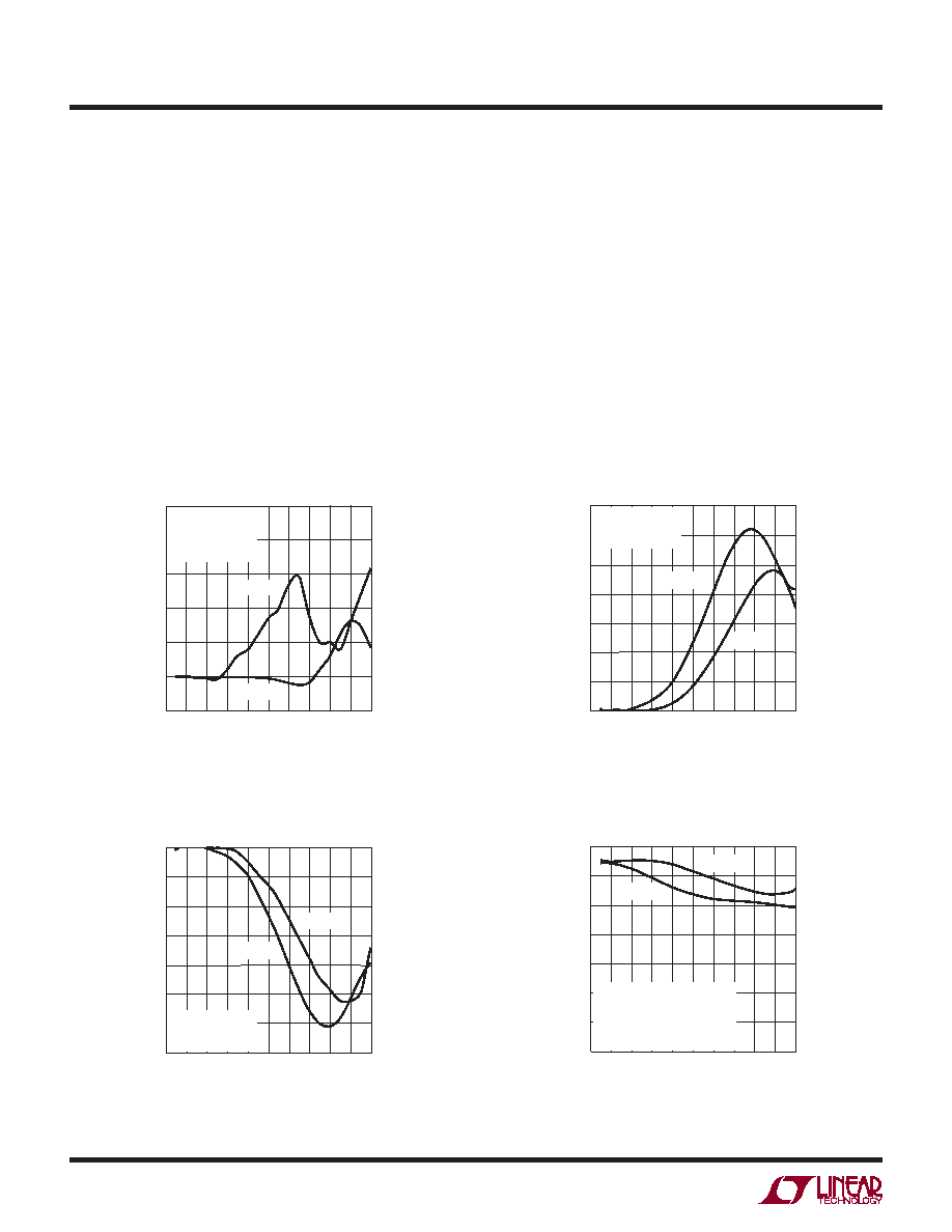
Figure 16. Offset Error vs Output Data Rate and Temperature
OUTPUT DATA RATE (READINGS/SEC)
–10
OFFSET
ERROR
(ppm
OF
V
REF
)
10
30
50
0
20
40
20
40
60
80
2483 F16
100
10
0
30
50
70
90
VIN(CM) = VREF(CM)
VCC = VREF = 5V
VIN = 0V
CA0/F0 = EXT CLOCK
TA = 85°C
TA = 25°C
output data rate. The increase in output rate is neverthe-
less accompanied by three potential effects, which must
be carefully considered.
First, a change in fEOSC will result in a proportional change
in the internal notch position and in a reduction of the
converter differential mode rejection at the power line fre-
quency.Inmanyapplications,thesubsequentperformance
degradation can be substantially reduced by relying upon
the LTC2483’s exceptional common mode rejection and by
carefully eliminating common mode to differential mode
conversion sources in the input circuit. The user should
avoid single-ended input filters and should maintain a
very high degree of matching and symmetry in the circuits
driving the IN+ and IN– pins.
Figure 17. +FS Error vs Output Data Rate and Temperature
OUTPUT DATA RATE (READINGS/SEC)
0
+FS
ERROR
(ppm
OF
V
REF
)
500
1500
2000
2500
3500
10
50
70
2483 F17
1000
3000
40
90 100
20 30
60
80
VIN(CM) = VREF(CM)
VCC = VREF = 5V
CA0/F0 = EXT CLOCK
TA = 85°C
TA = 25°C
Figure 18. –FS Error vs Output Data Rate and Temperature
OUTPUT DATA RATE (READINGS/SEC)
0
–3500
–FS
ERROR
(ppm
OF
V
REF
)
–3000
–2000
–1500
–1000
0
10
50
70
2483 F18
–2500
–500
40
90 100
20 30
60
80
VIN(CM) = VREF(CM)
VCC = VREF = 5V
CA0/F0 = EXT CLOCK
TA = 85°C
TA = 25°C
Figure 19. Resolution (NoiseRMS ≤ 1 LSB)
vs Output Data Rate and Temperature
OUTPUT DATA RATE (READINGS/SEC)
0
10
RESOLUTION
(BITS)
12
16
18
20
24
10
50
70
2483 F19
14
22
40
90 100
20 30
60
80
VIN(CM) = VREF(CM)
VCC = VREF = 5V
VIN = 0V
CA0/F0 = EXT CLOCK
RES = LOG 2 (VREF/NOISERMS)
TA = 85°C
TA = 25°C
相关PDF资料 |
PDF描述 |
|---|---|
| LTC2485CDD#TRPBF | IC ADC 24BIT I2C 10-DFN |
| LTC2487CDE#PBF | IC ADC 16BIT DELTA SIG 14-DFN |
| LTC2492IDE#TRPBF | IC ADC 24BIT DELTA SIG 14-DFN |
| LTC2493IDE#TRPBF | IC ADC 24BIT DELTA SIG 14-DFN |
| LTC2494IUHF#TRPBF | IC ADC 16BIT W/PGA 38-QFN |
相关代理商/技术参数 |
参数描述 |
|---|---|
| LTC2484CDD | 制造商:Linear Technology 功能描述:ADC Single Delta-Sigma 7.5sps 24-bit Serial 10-Pin DFN EP |
| LTC2484CDD#PBF | 功能描述:IC ADC 24BIT 10-DFN RoHS:是 类别:集成电路 (IC) >> 数据采集 - 模数转换器 系列:- 标准包装:1 系列:microPOWER™ 位数:8 采样率(每秒):1M 数据接口:串行,SPI? 转换器数目:1 功率耗散(最大):- 电压电源:模拟和数字 工作温度:-40°C ~ 125°C 安装类型:表面贴装 封装/外壳:24-VFQFN 裸露焊盘 供应商设备封装:24-VQFN 裸露焊盘(4x4) 包装:Digi-Reel® 输入数目和类型:8 个单端,单极 产品目录页面:892 (CN2011-ZH PDF) 其它名称:296-25851-6 |
| LTC2484CDD#TR | 制造商:Linear Technology 功能描述:ADC Single Delta-Sigma 7.5sps 24-bit Serial 10-Pin DFN EP T/R |
| LTC2484CDD#TRPBF | 功能描述:IC ADC 24BIT 10-DFN RoHS:是 类别:集成电路 (IC) >> 数据采集 - 模数转换器 系列:- 标准包装:2,500 系列:- 位数:16 采样率(每秒):15 数据接口:MICROWIRE?,串行,SPI? 转换器数目:1 功率耗散(最大):480µW 电压电源:单电源 工作温度:-40°C ~ 85°C 安装类型:表面贴装 封装/外壳:38-WFQFN 裸露焊盘 供应商设备封装:38-QFN(5x7) 包装:带卷 (TR) 输入数目和类型:16 个单端,双极;8 个差分,双极 配用:DC1011A-C-ND - BOARD DELTA SIGMA ADC LTC2494 |
| LTC2484IDD | 制造商:Linear Technology 功能描述:ADC Single Delta-Sigma 7.5sps 24-bit Serial 10-Pin DFN EP |
发布紧急采购,3分钟左右您将得到回复。