- 您现在的位置:买卖IC网 > PDF目录10354 > LTC2488CDE#TRPBF (Linear Technology)IC ADC 16BIT DELTA SIG 14-DFN PDF资料下载
参数资料
| 型号: | LTC2488CDE#TRPBF |
| 厂商: | Linear Technology |
| 文件页数: | 26/30页 |
| 文件大小: | 0K |
| 描述: | IC ADC 16BIT DELTA SIG 14-DFN |
| 标准包装: | 2,500 |
| 位数: | 16 |
| 采样率(每秒): | 6.9 |
| 数据接口: | MICROWIRE?,串行,SPI? |
| 转换器数目: | 1 |
| 功率耗散(最大): | 800µW |
| 电压电源: | 单电源 |
| 工作温度: | 0°C ~ 70°C |
| 安装类型: | 表面贴装 |
| 封装/外壳: | 14-WFDFN 裸露焊盘 |
| 供应商设备封装: | 14-DFN-EP(4x3) |
| 包装: | 带卷 (TR) |
| 输入数目和类型: | 4 个单端,双极;2 个差分,双极 |
| 配用: | DC1009A-B-ND - BOARD DELTA SIGMA ADC LTC2488 |
第1页第2页第3页第4页第5页第6页第7页第8页第9页第10页第11页第12页第13页第14页第15页第16页第17页第18页第19页第20页第21页第22页第23页第24页第25页当前第26页第27页第28页第29页第30页
LTC2488
5
2488fa
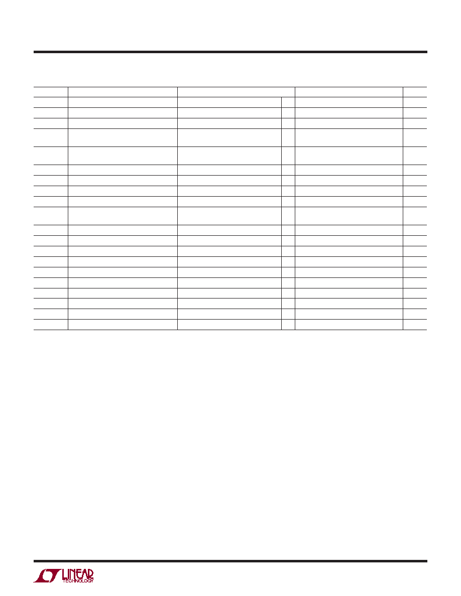
SYMBOL
PARAMETER
CONDITIONS
MIN
TYP
MAX
UNITS
fEOSC
External Oscillator Frequency Range
(Note 16)
●
10
4000
kHz
tHEO
External Oscillator High Period
●
0.125
100
μs
tLEO
External Oscillator Low Period
●
0.125
100
μs
tCONV
Conversion Time
Simultaneous 50Hz/60Hz
External Oscillator
●
144.1
146.9
41036/fEOSC (in kHz)
149.9
ms
fISCK
Internal SCK Frequency
Internal Oscillator (Notes 10, 17)
External Oscillator (Notes 10, 11, 15)
38.4
fEOSC/8
kHz
DISCK
Internal SCK Duty Cycle
(Notes 10, 17)
●
45
55
%
fESCK
External SCK Frequency Range
(Notes 10, 11, 15)
●
4000
kHz
tLESCK
External SCK Low Period
(Notes 10, 11, 15)
●
125
ns
tHESCK
External SCK High Period
(Notes 10, 11, 15)
●
125
ns
tDOUT_ISCK
Internal SCK 24-Bit Data Output Time
Internal Oscillator (Notes 10, 17)
External Oscillator (Notes 10, 11, 15)
●
0.61
0.625
192/fEOSC (in kHz)
0.64
ms
tDOUT_ESCK
External SCK 24-Bit Data Output Time
24/fESCK (in kHz)
ms
t1
CS↓ to SDO Low
●
0
200
ns
t2
CS↑ to SDO High Z
●
0
200
ns
t3
CS↓ to SCK↓
Internal SCK Mode
●
0
200
ns
t4
CS↓ to SCK↑
External SCK Mode
●
50
ns
tKQMAX
SCK↓ to SDO Valid
●
200
ns
tKQMIN
SDO Hold After SCK↓
(Note 5)
●
15
ns
t5
SCK Set-Up Before CS↓
●
50
ns
t7
SDI Setup Before SCK↑
(Note 5)
●
100
ns
t8
SDI Hold After SCK↑
(Note 5)
●
100
ns
DIGITAL INPUTS AND DIGITAL OUTPUTS The ● denotes the specications which apply over the
full operating temperature range, otherwise specications are at TA = 25°C. (Note 3)
Note 1: Stresses beyond those listed under Absolute Maximum Ratings may
cause permanent damage to the device. Exposure to any Absolute Maximum
Rating condition for extended periods may affect device reliability and lifetime.
Note 2: All voltage values are with respect to GND.
Note 3: Unless otherwise specied:
VCC = 2.7V to 5.5V
VREFCM = VREF/2, FS = 0.5VREF
VIN = IN+ – IN–, VIN(CM) = (IN+ – IN–)/2,
where IN+ and IN– are the selected input channels.
Note 4: Use internal conversion clock or external conversion clock source
with fEOSC = 307.2kHz unless other wise specied.
Note 5: Guaranteed by design, not subject to test.
Note 6: Integral nonlinearity is dened as the deviation of a code from a
straight line passing through the actual endpoints of the transfer curve.
The deviation is measured from the center of the quantization band.
Note 7: fEOSC = 256kHz ±2% (external oscillator).
Note 8: fEOSC = 307.2kHz ±2% (external oscillator).
Note 9: Simultaneous 50Hz/60Hz (internal oscillator) or fEOSC = 280kHz
±2% (external oscillator).
Note 10: The SCK can be congured in external SCK mode or internal SCK
mode. In external SCK mode, the SCK pin is used as a digital input and the
driving clock is fESCK. In the internal SCK mode, the SCK pin is used as a
digital output and the output clock signal during the data output is fISCK.
Note 11: The external oscillator is connected to the FO pin. The external
oscillator frequency, fEOSC, is expressed in kHz.
Note 12: The converter uses its internal oscillator.
Note 13: The output noise includes the contribution of the internal
calibration operations. VREF ≤ VCC.
Note 14: Guaranteed by design and test correlation.
Note 15: The converter is in external SCK mode of operation such that the
SCK pin is used as a digital input. The frequency of the clock signal driving
SCK during the data output is fESCK and is expressed in Hz.
Note 16: Refer to Applications Information section for performance vs
data rate graphs.
Note 17: The converter in internal SCK mode of operation such that the
SCK pin is used as a digital output.
Note 18: For VCC < 3V, VIH is 2.5V for pin fO.
相关PDF资料 |
PDF描述 |
|---|---|
| MAX9716EBL+TG45 | IC AMP AUDIO PWR 1.4W MONO 9UCSP |
| MS27497T16B99PA | CONN RCPT 23POS WALL MNT W/PINS |
| LTC1197CS8#TRPBF | IC A/DCONV 10BIT W/SHTDWN 8-SOIC |
| MS27473E12F35S | CONN PLUG 22POS STRAIGHT W/SCKT |
| LTC2436-1CGN#TRPBF | IC CONV A/D 16B 2CH DIFF 16SSOP |
相关代理商/技术参数 |
参数描述 |
|---|---|
| LTC2488IDE#PBF | 功能描述:IC ADC 16BIT DELTA SIG 14-DFN RoHS:是 类别:集成电路 (IC) >> 数据采集 - 模数转换器 系列:- 标准包装:1 系列:microPOWER™ 位数:8 采样率(每秒):1M 数据接口:串行,SPI? 转换器数目:1 功率耗散(最大):- 电压电源:模拟和数字 工作温度:-40°C ~ 125°C 安装类型:表面贴装 封装/外壳:24-VFQFN 裸露焊盘 供应商设备封装:24-VQFN 裸露焊盘(4x4) 包装:Digi-Reel® 输入数目和类型:8 个单端,单极 产品目录页面:892 (CN2011-ZH PDF) 其它名称:296-25851-6 |
| LTC2488IDE#TRPBF | 功能描述:IC ADC 16BIT DELTA SIG 14-DFN RoHS:是 类别:集成电路 (IC) >> 数据采集 - 模数转换器 系列:- 标准包装:2,500 系列:- 位数:16 采样率(每秒):15 数据接口:MICROWIRE?,串行,SPI? 转换器数目:1 功率耗散(最大):480µW 电压电源:单电源 工作温度:-40°C ~ 85°C 安装类型:表面贴装 封装/外壳:38-WFQFN 裸露焊盘 供应商设备封装:38-QFN(5x7) 包装:带卷 (TR) 输入数目和类型:16 个单端,双极;8 个差分,双极 配用:DC1011A-C-ND - BOARD DELTA SIGMA ADC LTC2494 |
| LTC2489CDE#PBF | 功能描述:IC ADC 16BIT DELTA SIG 14-DFN RoHS:是 类别:集成电路 (IC) >> 数据采集 - 模数转换器 系列:- 标准包装:2,500 系列:- 位数:16 采样率(每秒):15 数据接口:MICROWIRE?,串行,SPI? 转换器数目:1 功率耗散(最大):480µW 电压电源:单电源 工作温度:-40°C ~ 85°C 安装类型:表面贴装 封装/外壳:38-WFQFN 裸露焊盘 供应商设备封装:38-QFN(5x7) 包装:带卷 (TR) 输入数目和类型:16 个单端,双极;8 个差分,双极 配用:DC1011A-C-ND - BOARD DELTA SIGMA ADC LTC2494 |
| LTC2489CDE#TRPBF | 功能描述:IC ADC 16BIT DELTA SIG 14-DFN RoHS:是 类别:集成电路 (IC) >> 数据采集 - 模数转换器 系列:- 标准包装:2,500 系列:- 位数:16 采样率(每秒):15 数据接口:MICROWIRE?,串行,SPI? 转换器数目:1 功率耗散(最大):480µW 电压电源:单电源 工作温度:-40°C ~ 85°C 安装类型:表面贴装 封装/外壳:38-WFQFN 裸露焊盘 供应商设备封装:38-QFN(5x7) 包装:带卷 (TR) 输入数目和类型:16 个单端,双极;8 个差分,双极 配用:DC1011A-C-ND - BOARD DELTA SIGMA ADC LTC2494 |
| LTC2489IDE | 制造商:Linear Technology 功能描述:ADC Single Delta-Sigma 7.5sps 16-bit Serial 14-Pin DFN EP |
发布紧急采购,3分钟左右您将得到回复。