- 您现在的位置:买卖IC网 > PDF目录2006 > LTC2496IUHF#TRPBF (Linear Technology)IC ADC 16BIT DELTA SIG 38-QFN PDF资料下载
参数资料
| 型号: | LTC2496IUHF#TRPBF |
| 厂商: | Linear Technology |
| 文件页数: | 3/32页 |
| 文件大小: | 0K |
| 描述: | IC ADC 16BIT DELTA SIG 38-QFN |
| 标准包装: | 2,500 |
| 位数: | 16 |
| 采样率(每秒): | 6.9 |
| 数据接口: | MICROWIRE?,串行,SPI? |
| 转换器数目: | 1 |
| 功率耗散(最大): | 800µW |
| 电压电源: | 单电源 |
| 工作温度: | -40°C ~ 85°C |
| 安装类型: | 表面贴装 |
| 封装/外壳: | 38-WFQFN 裸露焊盘 |
| 供应商设备封装: | 38-QFN(5x7) |
| 包装: | 带卷 (TR) |
| 输入数目和类型: | 16 个单端,双极;8 个差分,双极 |
| 配用: | DC1011A-B-ND - BOARD DELTA SIGMA ADC LTC2496 |
第1页第2页当前第3页第4页第5页第6页第7页第8页第9页第10页第11页第12页第13页第14页第15页第16页第17页第18页第19页第20页第21页第22页第23页第24页第25页第26页第27页第28页第29页第30页第31页第32页
LTC2496
2496fb
applicaTions inForMaTion
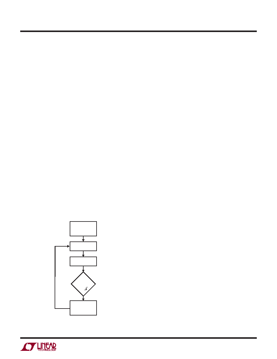
CONVERTER OPERATION
Converter Operation Cycle
The LTC2496 is a multi-channel, low power, delta-sigma
analog-to-digital converter with an easy to use 4-wire
interface and automatic differential input current can-
cellation. Its operation is made up of three states (See
Figure 2). The converter operating cycle begins with the
conversion, followed by the sleep state and ends with the
data input/output cycle. The 4-wire interface consists of
serial data output (SDO), serial clock (SCK), chip select
(CS) and serial data input (SDI).The interface, timing,
operation cycle, and data output format is compatible with
Linear’s entire family of
ΔΣ converters.
Initially, at power up, the LTC2496 performs a conversion.
Once the conversion is complete, the device enters the
sleep state. While in this sleep state, if CS is HIGH, power
consumption is reduced by two orders of magnitude. The
part remains in the sleep state as long as CS is HIGH. The
conversionresultisheldindefinitelyinastaticshiftregister
while the part is in the sleep state.
Once CS is pulled LOW, the device powers up, exits the
sleep mode, and enters the data input/output state. If CS
is brought HIGH before the first rising edge of SCK, the
device returns to the sleep state and the power is reduced.
If CS is brought HIGH after the first rising edge of SCK, the
data output cycle is aborted and a new conversion cycle
begins. The data output corresponds to the conversion
just completed. This result is shifted out on the serial
data output pin (SDO) under the control of the serial
clock pin (SCK). Data is updated on the falling edge of
SCK allowing the user to reliably latch data on the rising
edge of SCK (See Figure 3). The channel selection data for
the next conversion is also loaded into the device at this
time. Data is loaded from the serial data input pin (SDI)
on each rising edge of SCK. The data input/output cycle is
concluded once 24 bits are read out of the ADC or when
CS is brought HIGH. The device automatically initiates a
new conversion and the cycle repeats.
ThroughtimingcontroloftheCSandSCKpins,theLTC2496
offers several flexible modes of operation (internal or
external SCK and free-running conversion modes). These
various modes do not require programming and do not
disturbthecyclicoperationdescribedabove.Thesemodes
of operation are described in detail in the Serial Interface
Timing Modes section.
Ease of Use
The LTC2496 data output has no latency, filter settling
delay or redundant data associated with the conversion
cycle. There is a one-to-one correspondence between the
conversion and the output data. Therefore, multiplexing
multipleanaloginputsisstraightforward.Eachconversion,
immediately following a newly selected input, is valid and
accurate to the full specifications of the device.
The LTC2496 automatically performs offset and full scale
calibration every conversion cycle independent of the
input channel selected. This calibration is transparent to
the user and has no effect with the operation cycle de-
scribed above. The advantage of continuous calibration
is extreme stability of offset and full-scale readings with
respect to time, supply voltage variation, input channel,
and temperature drift.
Easy Drive Input Current Cancellation
The LTC2496 combines a high precision delta-sigma ADC
with an automatic, differential, input current cancellation
Figure 2. LTC2496 State Transition Diagram
CONVERT
SLEEP
CHANNEL SELECT
DATA OUTPUT
POWER UP
IN+= CH0, IN–= CH1
2496 F02
CS = LOW
AND
SCK
相关PDF资料 |
PDF描述 |
|---|---|
| LTC2498IUHF#TRPBF | IC ADC 24BIT 16CH 38-QFN |
| LTC2600IUFD#PBF | IC DAC OCTAL R-R 16BIT 20-QFN |
| LTC2602IMS8#TRPBF | IC DAC 16BIT DUAL R-R VOUT 8MSOP |
| LTC2604IGN-1#TRPBF | IC DAC 16BIT QUAD R-R OUT 16SSOP |
| LTC2605IGN-1#TRPBF | IC DAC 16BIT OCT I2C 16-SSOP |
相关代理商/技术参数 |
参数描述 |
|---|---|
| LTC2497CUHF#PBF | 功能描述:IC ADC 16BIT W/PGA 38-QFN RoHS:是 类别:集成电路 (IC) >> 数据采集 - 模数转换器 系列:- 标准包装:1 系列:microPOWER™ 位数:8 采样率(每秒):1M 数据接口:串行,SPI? 转换器数目:1 功率耗散(最大):- 电压电源:模拟和数字 工作温度:-40°C ~ 125°C 安装类型:表面贴装 封装/外壳:24-VFQFN 裸露焊盘 供应商设备封装:24-VQFN 裸露焊盘(4x4) 包装:Digi-Reel® 输入数目和类型:8 个单端,单极 产品目录页面:892 (CN2011-ZH PDF) 其它名称:296-25851-6 |
| LTC2497CUHF#TRPBF | 功能描述:IC ADC 16BIT W/PGA 38-QFN RoHS:是 类别:集成电路 (IC) >> 数据采集 - 模数转换器 系列:- 标准包装:2,500 系列:- 位数:16 采样率(每秒):15 数据接口:MICROWIRE?,串行,SPI? 转换器数目:1 功率耗散(最大):480µW 电压电源:单电源 工作温度:-40°C ~ 85°C 安装类型:表面贴装 封装/外壳:38-WFQFN 裸露焊盘 供应商设备封装:38-QFN(5x7) 包装:带卷 (TR) 输入数目和类型:16 个单端,双极;8 个差分,双极 配用:DC1011A-C-ND - BOARD DELTA SIGMA ADC LTC2494 |
| LTC2497IUHF#PBF | 功能描述:IC ADC 16BIT W/PGA 38-QFN RoHS:是 类别:集成电路 (IC) >> 数据采集 - 模数转换器 系列:- 标准包装:2,500 系列:- 位数:16 采样率(每秒):15 数据接口:MICROWIRE?,串行,SPI? 转换器数目:1 功率耗散(最大):480µW 电压电源:单电源 工作温度:-40°C ~ 85°C 安装类型:表面贴装 封装/外壳:38-WFQFN 裸露焊盘 供应商设备封装:38-QFN(5x7) 包装:带卷 (TR) 输入数目和类型:16 个单端,双极;8 个差分,双极 配用:DC1011A-C-ND - BOARD DELTA SIGMA ADC LTC2494 |
| LTC2497IUHF#TRPBF | 功能描述:IC ADC 16BIT W/PGA 38-QFN RoHS:是 类别:集成电路 (IC) >> 数据采集 - 模数转换器 系列:- 标准包装:2,500 系列:- 位数:16 采样率(每秒):15 数据接口:MICROWIRE?,串行,SPI? 转换器数目:1 功率耗散(最大):480µW 电压电源:单电源 工作温度:-40°C ~ 85°C 安装类型:表面贴装 封装/外壳:38-WFQFN 裸露焊盘 供应商设备封装:38-QFN(5x7) 包装:带卷 (TR) 输入数目和类型:16 个单端,双极;8 个差分,双极 配用:DC1011A-C-ND - BOARD DELTA SIGMA ADC LTC2494 |
| LTC2498CUHF | 制造商:Linear Technology 功能描述:ADC Single Delta-Sigma 7.5sps 24-bit Serial 38-Pin QFN EP |
发布紧急采购,3分钟左右您将得到回复。