- 您现在的位置:买卖IC网 > PDF目录8973 > LTC2614IGN-1#PBF (Linear Technology)IC DAC 14BIT QUAD R-R 16-SSOP PDF资料下载
参数资料
| 型号: | LTC2614IGN-1#PBF |
| 厂商: | Linear Technology |
| 文件页数: | 6/16页 |
| 文件大小: | 0K |
| 描述: | IC DAC 14BIT QUAD R-R 16-SSOP |
| 标准包装: | 100 |
| 设置时间: | 9µs |
| 位数: | 14 |
| 数据接口: | 串行 |
| 转换器数目: | 4 |
| 电压电源: | 单电源 |
| 功率耗散(最大): | 10mW |
| 工作温度: | -40°C ~ 85°C |
| 安装类型: | 表面贴装 |
| 封装/外壳: | 16-SSOP(0.154",3.90mm 宽) |
| 供应商设备封装: | 16-SSOP |
| 包装: | 管件 |
| 输出数目和类型: | 4 电压,单极 |
| 采样率(每秒): | * |
| 产品目录页面: | 1351 (CN2011-ZH PDF) |
LTC2604/LTC2614/LTC2624
14
2604fd
OPERATION
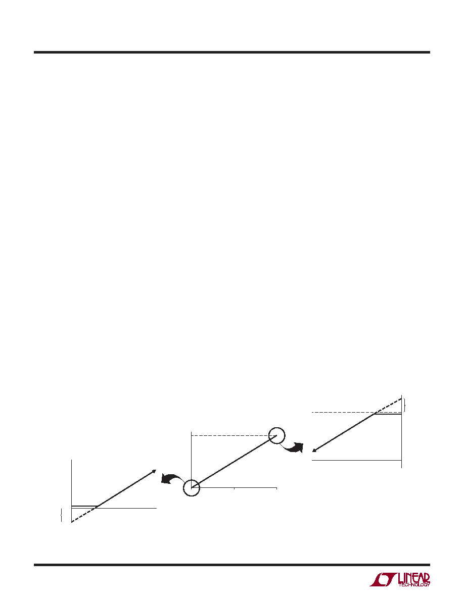
2600 F03
INPUT CODE
OUTPUT
VOLTAGE
NEGATIVE
OFFSET
0V
32,768
0
65,535
INPUT CODE
OUTPUT
VOLTAGE
VREF = VCC
INPUT CODE
OUTPUT
VOLTAGE
POSITIVE
FSE
Figure 3. Effects of Rail-to-Rail Operation On a DAC Transfer Curve. (a) Overall Transfer Function (b) Effect
of Negative Offset for Codes Near Zero Scale (c) Effect of Positive Full-Scale Error for Codes Near Full Scale
(b)
(a)
(c)
DC output impedance is equivalent to load regulation, and
may be derived from it by simply calculating a change in
units from LSB/mA to Ohms. The ampliers’ DC output
impedance is 0.025Ω when driving a load well away from
the rails.
When drawing a load current from either rail, the output
voltage headroom with respect to that rail is limited by
the 30Ω typical channel resistance of the output devices;
e.g., when sinking 1mA, the minimum output voltage =
30Ω 1mA = 30mV. See the graph Headroom at Rails vs
Output Current in the Typical Performance Characteristics
section.
The ampliers are stable driving capacitive loads of up
to 1000pF.
Board Layout
The excellent load regulation and DC crosstalk performance
of these devices is achieved in part by keeping “signal”
and “power” grounds separate.
The PC board should have separate areas for the analog
and digital sections of the circuit. This keeps digital signals
away from sensitive analog signals and facilitates the use
of separate digital and analog ground planes which have
minimal capacitive and resistive interaction with each
other.
Digital and analog ground planes should be joined at only
one point, establishing a system star ground as close to
the device’s ground pin as possible. Ideally, the analog
ground plane should be located on the component side of
the board, and should be allowed to run under the part to
shield it from noise. Analog ground should be a continuous
and uninterrupted plane, except for necessary lead pads
and vias, with signal traces on another layer.
The GND pin functions as a return path for power sup-
ply currents in the device and should be connected to
analog ground. Resistance from the GND pin to system
star ground should be as low as possible. When a zero
scale DAC output voltage of zero is desired, the REFLO pin
(pin 2) should be connected to system star ground.
Rail-to-Rail Output Considerations
In any rail-to-rail voltage output device, the output is limited
to voltages within the supply range.
Since the analog outputs of the device cannot go below
ground, they may limit for the lowest codes as shown in
Figure 3b. Similarly, limiting can occur near full scale when
the REF pins are tied to VCC. If REF x = VCC and the DAC
full-scale error (FSE) is positive, the output for the highest
codes limits at VCC as shown in Figure 3c. No full-scale
limiting can occur if REF x is less than VCC – FSE.
Offset and linearity are dened and tested over the region
of the DAC transfer function where no output limiting
can occur.
相关PDF资料 |
PDF描述 |
|---|---|
| MS3124E16-8S | CONN RCPT 8POS JAM NUT W/SCKT |
| ICS843004AGI-01LFT | IC SYNTHESIZER LVPECL 24-TSSOP |
| VE-JTY-MZ-F3 | CONVERTER MOD DC/DC 3.3V 16.5W |
| AD7243ARZ | IC DAC 12BIT W/AMP W/REF 16-SOIC |
| MS27508E24B4PA | CONN RCPT 56POS BOX MNT W/PINS |
相关代理商/技术参数 |
参数描述 |
|---|---|
| LTC2615CGN#PBF | 功能描述:IC DAC 14BIT R-R OCT 16SSOP RoHS:是 类别:集成电路 (IC) >> 数据采集 - 数模转换器 系列:- 产品培训模块:Data Converter Fundamentals DAC Architectures 标准包装:750 系列:- 设置时间:7µs 位数:16 数据接口:并联 转换器数目:1 电压电源:双 ± 功率耗散(最大):100mW 工作温度:0°C ~ 70°C 安装类型:表面贴装 封装/外壳:28-LCC(J 形引线) 供应商设备封装:28-PLCC(11.51x11.51) 包装:带卷 (TR) 输出数目和类型:1 电压,单极;1 电压,双极 采样率(每秒):143k |
| LTC2615CGN#TRPBF | 功能描述:IC DAC 14BIT R-R OCT 16SSOP RoHS:是 类别:集成电路 (IC) >> 数据采集 - 数模转换器 系列:- 标准包装:2,400 系列:- 设置时间:- 位数:18 数据接口:串行 转换器数目:3 电压电源:模拟和数字 功率耗散(最大):- 工作温度:-40°C ~ 85°C 安装类型:表面贴装 封装/外壳:36-TFBGA 供应商设备封装:36-TFBGA 包装:带卷 (TR) 输出数目和类型:* 采样率(每秒):* |
| LTC2615CGN-1#PBF | 功能描述:IC DAC 14BIT R-R OCT 16SSOP RoHS:是 类别:集成电路 (IC) >> 数据采集 - 数模转换器 系列:- 产品培训模块:Data Converter Fundamentals DAC Architectures 标准包装:750 系列:- 设置时间:7µs 位数:16 数据接口:并联 转换器数目:1 电压电源:双 ± 功率耗散(最大):100mW 工作温度:0°C ~ 70°C 安装类型:表面贴装 封装/外壳:28-LCC(J 形引线) 供应商设备封装:28-PLCC(11.51x11.51) 包装:带卷 (TR) 输出数目和类型:1 电压,单极;1 电压,双极 采样率(每秒):143k |
| LTC2615CGN-1#TRPBF | 功能描述:IC DAC 14BIT R-R OCT 16SSOP RoHS:是 类别:集成电路 (IC) >> 数据采集 - 数模转换器 系列:- 产品培训模块:Data Converter Fundamentals DAC Architectures 标准包装:750 系列:- 设置时间:7µs 位数:16 数据接口:并联 转换器数目:1 电压电源:双 ± 功率耗散(最大):100mW 工作温度:0°C ~ 70°C 安装类型:表面贴装 封装/外壳:28-LCC(J 形引线) 供应商设备封装:28-PLCC(11.51x11.51) 包装:带卷 (TR) 输出数目和类型:1 电压,单极;1 电压,双极 采样率(每秒):143k |
| LTC2615IGN#PBF | 功能描述:IC DAC 14BIT R-R OCT 16SSOP RoHS:是 类别:集成电路 (IC) >> 数据采集 - 数模转换器 系列:- 标准包装:1 系列:- 设置时间:4.5µs 位数:12 数据接口:串行,SPI? 转换器数目:1 电压电源:单电源 功率耗散(最大):- 工作温度:-40°C ~ 125°C 安装类型:表面贴装 封装/外壳:8-SOIC(0.154",3.90mm 宽) 供应商设备封装:8-SOICN 包装:剪切带 (CT) 输出数目和类型:1 电压,单极;1 电压,双极 采样率(每秒):* 其它名称:MCP4921T-E/SNCTMCP4921T-E/SNRCTMCP4921T-E/SNRCT-ND |
发布紧急采购,3分钟左右您将得到回复。