- 您现在的位置:买卖IC网 > PDF目录8735 > LTC2616CDD-1#TRPBF (Linear Technology)IC DAC 14BIT I2C V-OUT 10-DFN PDF资料下载
参数资料
| 型号: | LTC2616CDD-1#TRPBF |
| 厂商: | Linear Technology |
| 文件页数: | 6/20页 |
| 文件大小: | 0K |
| 描述: | IC DAC 14BIT I2C V-OUT 10-DFN |
| 标准包装: | 2,500 |
| 设置时间: | 9µs |
| 位数: | 14 |
| 数据接口: | I²C |
| 转换器数目: | 1 |
| 电压电源: | 单电源 |
| 功率耗散(最大): | 810µW |
| 工作温度: | 0°C ~ 70°C |
| 安装类型: | 表面贴装 |
| 封装/外壳: | 10-WFDFN 裸露焊盘 |
| 供应商设备封装: | 10-DFN(3x3) |
| 包装: | 带卷 (TR) |
| 输出数目和类型: | 1 电压,单极 |
| 采样率(每秒): | * |
LTC2606/LTC2616/LTC2626
14
26061626fb
OPERATION
Chip Address
The state of CA0, CA1 and CA2 decides the slave address
of the part. The pins CA0, CA1 and CA2 can be each set
to any one of three states: VCC, GND or oat. This results
in 27 selectable addresses for the part. The slave address
assignments are shown in Table 1.
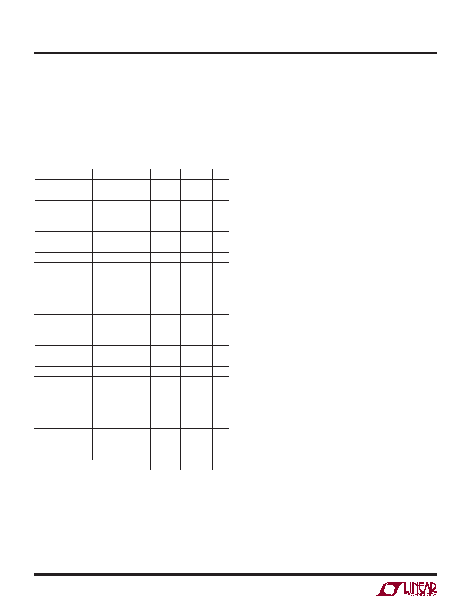
Table 1. Slave Address Map
CA2
CA1
CA0
A6
A5
A4
A3
A2
A1
A0
GND
0
1
0
GND
FLOAT
0
1
0
1
GND
VCC
00
1
0
1
0
GND
FLOAT
GND
0
1
0
1
GND
FLOAT
0
1
0
GND
FLOAT
VCC
01
0
1
GND
VCC
GND
0
1
0
1
0
GND
VCC
FLOAT
0
1
0
1
GND
VCC
01
1
0
FLOAT
GND
0
1
0
1
FLOAT
GND
FLOAT
0
1
0
1
0
FLOAT
GND
VCC
01
1
0
1
FLOAT
GND
1
0
FLOAT
1
0
1
FLOAT
VCC
10
0
1
0
FLOAT
VCC
GND
1
0
1
FLOAT
VCC
FLOAT
1
0
1
0
FLOAT
VCC
10
1
0
1
VCC
GND
1
0
1
0
1
0
VCC
GND
FLOAT
1
0
1
0
1
VCC
GND
VCC
11
0
VCC
FLOAT
GND
1
0
1
VCC
FLOAT
1
0
1
0
VCC
FLOAT
VCC
11
0
1
VCC
GND
1
0
VCC
FLOAT
1
0
1
VCC
11
1
0
1
0
GLOBAL ADDRESS
1
0
1
In addition to the address selected by the address pins,
the parts also respond to a global address. This address
allows a common write to all LTC2606, LTC2616 and
LTC2626 parts to be accomplished with one 3-byte write
transaction on the I2C bus. The global address is a 7-bit
on-chip hardwired address and is not selectable by CA0,
CA1 and CA2.
The addresses corresponding to the states of CA0, CA1
and CA2 and the global address are shown in Table 1. The
maximum capacitive load allowed on the address pins
(CA0, CA1 and CA2) is 10pF, as these pins are driven during
address detection to determine if they are oating.
Write Word Protocol
The master initiates communication with the LTC2606/
LTC2616/LTC2626 with a START condition and a 7-bit slave
address followed by the Write bit (W) = 0. The LTC2606/
LTC2616/LTC2626 acknowledges by pulling the SDA pin
low at the 9th clock if the 7-bit slave address matches the
address of the parts (set by CA0, CA1 and CA2) or the
global address. The master then transmits three bytes of
data. The LTC2606/LTC2616/LTC2626 acknowledges each
byte of data by pulling the SDA line low at the 9th clock of
each data byte transmission. After receiving three complete
bytes of data, the LTC2606/LTC2616/LTC2626 executes the
command specied in the 24-bit input word.
If more than three data bytes are transmitted after a valid
7-bit slave address, the LTC2606/LTC2616/LTC2626 do not
acknowledge the extra bytes of data (SDA is high during
the 9th clock).
The format of the three data bytes is shown in Figure 3.
The rst byte of the input word consists of the 4-bit com-
mand and four don’t care bits. The next two bytes consist
of the 16-bit data word. The 16-bit data word consists of
the 16-, 14- or 12-bit input code, MSB to LSB, followed by
0, 2 or 4 don’t care bits (LTC2606, LTC2616 and LTC2626
respectively). A typical LTC2606 write transaction is shown
in Figure 4.
The command assignments (C3-C0) are shown in Table 2.
The rst four commands in the table consist of write and
update operations. A write operation loads a 16-bit data
word from the 32-bit shift register into the input register.
In an update operation, the data word is copied from the
input register to the DAC register and converted to an
analog voltage at the DAC output. The update operation
also powers up the DAC if it had been in power-down
mode. The data path and registers are shown in the Block
Diagram.
相关PDF资料 |
PDF描述 |
|---|---|
| LTC2626IDD-1#TRPBF | IC DAC 12BIT I2C V-OUT 10-DFN |
| VI-B50-MX | CONVERTER MOD DC/DC 5V 75W |
| VI-2WW-MW-F3 | CONVERTER MOD DC/DC 5.5V 100W |
| AD5428YRU-REEL | IC DAC 8BIT MULTIPLYING 20-TSSOP |
| VI-B10-MX | CONVERTER MOD DC/DC 5V 75W |
相关代理商/技术参数 |
参数描述 |
|---|---|
| LTC2616IDD#PBF | 功能描述:IC DAC 14BIT I2C V-OUT 10-DFN RoHS:是 类别:集成电路 (IC) >> 数据采集 - 数模转换器 系列:- 产品培训模块:LTC263x 12-, 10-, and 8-Bit VOUT DAC Family 特色产品:LTC2636 - Octal 12-/10-/8-Bit SPI VOUT DACs with 10ppm/°C Reference 标准包装:91 系列:- 设置时间:4µs 位数:10 数据接口:MICROWIRE?,串行,SPI? 转换器数目:8 电压电源:单电源 功率耗散(最大):2.7mW 工作温度:-40°C ~ 85°C 安装类型:表面贴装 封装/外壳:14-WFDFN 裸露焊盘 供应商设备封装:14-DFN-EP(4x3) 包装:管件 输出数目和类型:8 电压,单极 采样率(每秒):* |
| LTC2616IDD#TRPBF | 功能描述:IC DAC 14BIT I2C V-OUT 10-DFN RoHS:是 类别:集成电路 (IC) >> 数据采集 - 数模转换器 系列:- 产品培训模块:LTC263x 12-, 10-, and 8-Bit VOUT DAC Family 特色产品:LTC2636 - Octal 12-/10-/8-Bit SPI VOUT DACs with 10ppm/°C Reference 标准包装:91 系列:- 设置时间:4µs 位数:10 数据接口:MICROWIRE?,串行,SPI? 转换器数目:8 电压电源:单电源 功率耗散(最大):2.7mW 工作温度:-40°C ~ 85°C 安装类型:表面贴装 封装/外壳:14-WFDFN 裸露焊盘 供应商设备封装:14-DFN-EP(4x3) 包装:管件 输出数目和类型:8 电压,单极 采样率(每秒):* |
| LTC2616IDD-1 | 制造商:Linear Technology 功能描述:DAC 1-CH 14-bit 10-Pin DFN EP |
| LTC2616IDD-1#PBF | 功能描述:IC DAC 14BIT I2C V-OUT 10-DFN RoHS:是 类别:集成电路 (IC) >> 数据采集 - 数模转换器 系列:- 产品培训模块:LTC263x 12-, 10-, and 8-Bit VOUT DAC Family 特色产品:LTC2636 - Octal 12-/10-/8-Bit SPI VOUT DACs with 10ppm/°C Reference 标准包装:91 系列:- 设置时间:4µs 位数:10 数据接口:MICROWIRE?,串行,SPI? 转换器数目:8 电压电源:单电源 功率耗散(最大):2.7mW 工作温度:-40°C ~ 85°C 安装类型:表面贴装 封装/外壳:14-WFDFN 裸露焊盘 供应商设备封装:14-DFN-EP(4x3) 包装:管件 输出数目和类型:8 电压,单极 采样率(每秒):* |
| LTC2616IDD-1#TRPBF | 功能描述:IC DAC 14BIT I2C V-OUT 10-DFN RoHS:是 类别:集成电路 (IC) >> 数据采集 - 数模转换器 系列:- 产品培训模块:LTC263x 12-, 10-, and 8-Bit VOUT DAC Family 特色产品:LTC2636 - Octal 12-/10-/8-Bit SPI VOUT DACs with 10ppm/°C Reference 标准包装:91 系列:- 设置时间:4µs 位数:10 数据接口:MICROWIRE?,串行,SPI? 转换器数目:8 电压电源:单电源 功率耗散(最大):2.7mW 工作温度:-40°C ~ 85°C 安装类型:表面贴装 封装/外壳:14-WFDFN 裸露焊盘 供应商设备封装:14-DFN-EP(4x3) 包装:管件 输出数目和类型:8 电压,单极 采样率(每秒):* |
发布紧急采购,3分钟左右您将得到回复。