参数资料
| 型号: | LTC2616IDD#PBF |
| 厂商: | Linear Technology |
| 文件页数: | 7/20页 |
| 文件大小: | 0K |
| 描述: | IC DAC 14BIT I2C V-OUT 10-DFN |
| 标准包装: | 121 |
| 设置时间: | 9µs |
| 位数: | 14 |
| 数据接口: | I²C |
| 转换器数目: | 1 |
| 电压电源: | 单电源 |
| 功率耗散(最大): | 810µW |
| 工作温度: | -40°C ~ 85°C |
| 安装类型: | 表面贴装 |
| 封装/外壳: | 10-WFDFN 裸露焊盘 |
| 供应商设备封装: | 10-DFN(3x3) |
| 包装: | 管件 |
| 输出数目和类型: | 1 电压,单极 |
| 采样率(每秒): | * |
LTC2606/LTC2616/LTC2626
15
26061626fb
OPERATION
Power-Down Mode
For power-constrained applications, power-down mode
can be used to reduce the supply current whenever the
DAC output is not needed. When in power-down, the buffer
amplier, bias circuit and reference input is disabled and
draws essentially zero current. The DAC output is put into a
high impedance state, and the output pin is passively pulled
to ground through 90k resistors. Input- and DAC-register
contents are not disturbed during power-down.
Table 2
COMMAND*
C3
C2 C1 C0
0
Write to Input Register
0
1
Update (Power Up) DAC Register
0
1
Write to and Update (Power Up)
0
1
0
Power Down
1
No Operation
*Command codes not shown are reserved and should not be used.
The DAC channel can be put into power-down mode by
using command 0100b. The 16-bit data word is ignored.
The supply and reference currents are reduced to almost
zero when the DAC is powered down; the effective resis-
tance at REF becomes a high impedance input (typically
>1GΩ).
Normal operation can be resumed by executing any com-
mand which includes a DAC update, as shown in Table 2 or
performing an asychronous update (LDAC) as described
in the next section. The DAC is powered up as its voltage
output is updated. When the DAC in powered-down state
is powered up and updated, normal settling is delayed. The
main bias generation circuit block has been automatically
shut down in addition to the DAC amplier and reference
input and so the power-up delay time is:
12μs (for VCC = 5V) or 30μs (for VCC = 3V)
Asynchronous DAC Update Using LDAC
In addition to the update commands shown in Table 2,
the LDAC pin asynchronously updates the DAC register
with the contents of the input register. Asynchronous
update is disabled when the input word is being clocked
into the part.
If a complete input word has been written to the part, a low
on the LDAC pin causes the DAC register to be updated
with the contents of the input register.
If the input word is being written to the part, a low going
pulse on the LDAC pin before the completion of three bytes
of data powers up the DAC but does not cause the output
to be updated. If LDAC remains low after a complete input
word has been written to the part, then LDAC is recognized,
the command specied in the 24-bit word just transferred
is executed and the DAC output is updated.
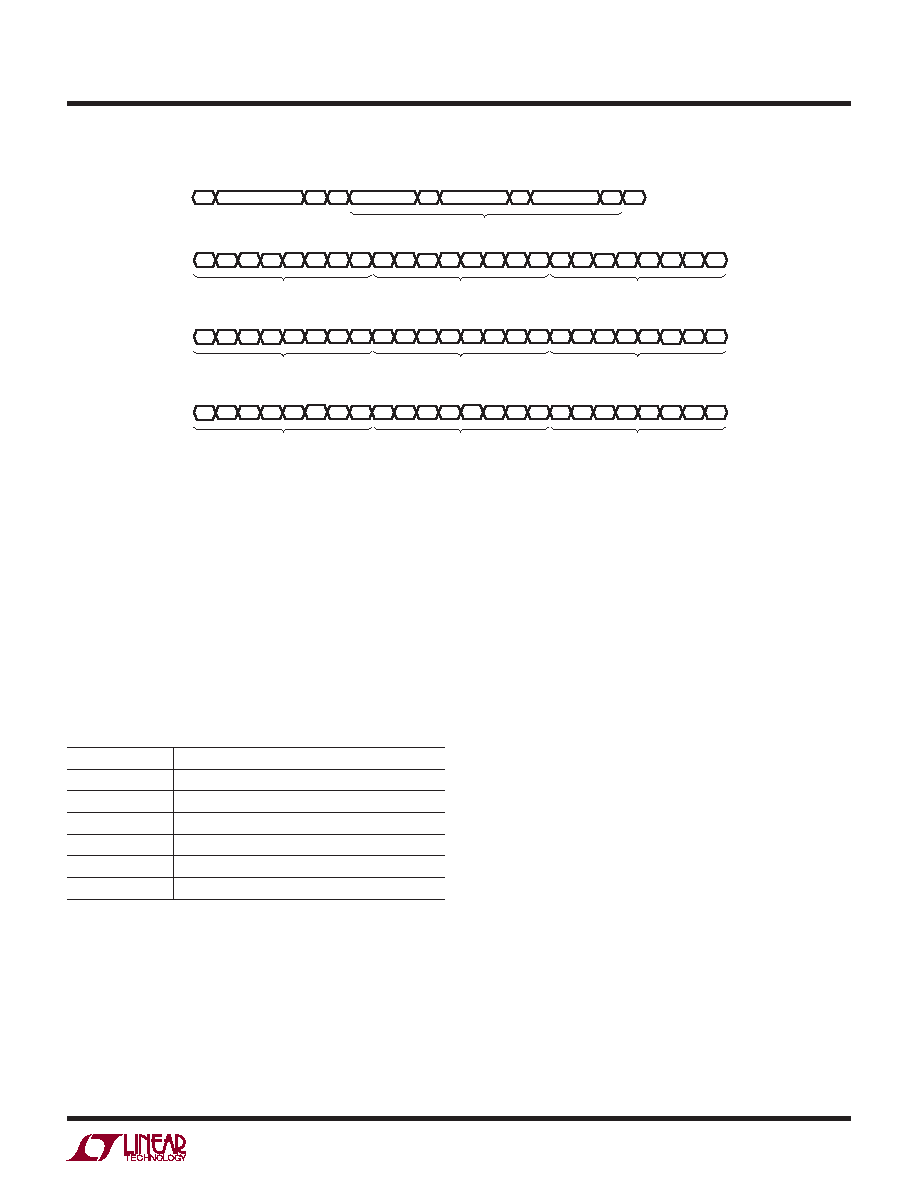
Figure 3
C3
1ST DATA BYTE
Input Word (LTC2606)
Write Word Protocol for LTC2606/LTC2616/LTC1626
C2
C1
C0
X
D13
D14
D15
S
WA
SLAVE ADDRESS
1ST DATA BYTE
D12 D11 D10 D9
D8
D7 D6
D5
D4
D3
D2
D1 D0
A
2ND DATA BYTE
A
3RD DATA BYTE
A
P
2606 F03
2ND DATA BYTE
INPUT WORD
3RD DATA BYTE
C3
1ST DATA BYTE
Input Word (LTC2616)
C2
C1
C0
X
D11
D12
D13
D10 D9
D8
D7
D6
D5 D4
D3
D2
D1
D0
X
2ND DATA BYTE
3RD DATA BYTE
C3
1ST DATA BYTE
Input Word (LTC2626)
C2
C1
C0
X
D9
D10
D11
D8
D7
D6
D5
D4
D3 D2
D1
D0
X
2ND DATA BYTE
3RD DATA BYTE
相关PDF资料 |
PDF描述 |
|---|---|
| VI-2NZ-MX-F4 | CONVERTER MOD DC/DC 2V 30W |
| V24A12H400B3 | CONVERTER MOD DC/DC 12V 400W |
| V24A12H400B2 | CONVERTER MOD DC/DC 12V 400W |
| V24A12H400B | CONVERTER MOD DC/DC 12V 400W |
| LTC2616IDD#TRPBF | IC DAC 14BIT I2C V-OUT 10-DFN |
相关代理商/技术参数 |
参数描述 |
|---|---|
| LTC2617CDE#PBF | 功能描述:IC DAC 14BIT R-R I2C 12-DFN RoHS:是 类别:集成电路 (IC) >> 数据采集 - 数模转换器 系列:- 产品培训模块:LTC263x 12-, 10-, and 8-Bit VOUT DAC Family 特色产品:LTC2636 - Octal 12-/10-/8-Bit SPI VOUT DACs with 10ppm/°C Reference 标准包装:91 系列:- 设置时间:4µs 位数:10 数据接口:MICROWIRE?,串行,SPI? 转换器数目:8 电压电源:单电源 功率耗散(最大):2.7mW 工作温度:-40°C ~ 85°C 安装类型:表面贴装 封装/外壳:14-WFDFN 裸露焊盘 供应商设备封装:14-DFN-EP(4x3) 包装:管件 输出数目和类型:8 电压,单极 采样率(每秒):* |
| LTC2617CDE#TRPBF | 功能描述:IC DAC 14BIT R-R I2C 12-DFN RoHS:是 类别:集成电路 (IC) >> 数据采集 - 数模转换器 系列:- 产品培训模块:LTC263x 12-, 10-, and 8-Bit VOUT DAC Family 特色产品:LTC2636 - Octal 12-/10-/8-Bit SPI VOUT DACs with 10ppm/°C Reference 标准包装:91 系列:- 设置时间:4µs 位数:10 数据接口:MICROWIRE?,串行,SPI? 转换器数目:8 电压电源:单电源 功率耗散(最大):2.7mW 工作温度:-40°C ~ 85°C 安装类型:表面贴装 封装/外壳:14-WFDFN 裸露焊盘 供应商设备封装:14-DFN-EP(4x3) 包装:管件 输出数目和类型:8 电压,单极 采样率(每秒):* |
| LTC2617CDE-1#PBF | 功能描述:IC DAC 14BIT R-R I2C 12-DFN RoHS:是 类别:集成电路 (IC) >> 数据采集 - 数模转换器 系列:- 产品培训模块:LTC263x 12-, 10-, and 8-Bit VOUT DAC Family 特色产品:LTC2636 - Octal 12-/10-/8-Bit SPI VOUT DACs with 10ppm/°C Reference 标准包装:91 系列:- 设置时间:4µs 位数:10 数据接口:MICROWIRE?,串行,SPI? 转换器数目:8 电压电源:单电源 功率耗散(最大):2.7mW 工作温度:-40°C ~ 85°C 安装类型:表面贴装 封装/外壳:14-WFDFN 裸露焊盘 供应商设备封装:14-DFN-EP(4x3) 包装:管件 输出数目和类型:8 电压,单极 采样率(每秒):* |
| LTC2617CDE-1#TRPBF | 功能描述:IC DAC 14BIT R-R I2C 12-DFN RoHS:是 类别:集成电路 (IC) >> 数据采集 - 数模转换器 系列:- 标准包装:2,400 系列:- 设置时间:- 位数:18 数据接口:串行 转换器数目:3 电压电源:模拟和数字 功率耗散(最大):- 工作温度:-40°C ~ 85°C 安装类型:表面贴装 封装/外壳:36-TFBGA 供应商设备封装:36-TFBGA 包装:带卷 (TR) 输出数目和类型:* 采样率(每秒):* |
| LTC2617IDE#PBF | 功能描述:IC DAC 14BIT R-R I2C 12-DFN RoHS:是 类别:集成电路 (IC) >> 数据采集 - 数模转换器 系列:- 标准包装:47 系列:- 设置时间:2µs 位数:14 数据接口:并联 转换器数目:1 电压电源:单电源 功率耗散(最大):55µW 工作温度:-40°C ~ 85°C 安装类型:表面贴装 封装/外壳:28-SSOP(0.209",5.30mm 宽) 供应商设备封装:28-SSOP 包装:管件 输出数目和类型:1 电流,单极;1 电流,双极 采样率(每秒):* |
发布紧急采购,3分钟左右您将得到回复。