参数资料
| 型号: | LTC2617CDE-1#PBF |
| 厂商: | Linear Technology |
| 文件页数: | 2/20页 |
| 文件大小: | 0K |
| 描述: | IC DAC 14BIT R-R I2C 12-DFN |
| 标准包装: | 91 |
| 设置时间: | 9µs |
| 位数: | 14 |
| 数据接口: | I²C |
| 转换器数目: | 2 |
| 电压电源: | 单电源 |
| 功率耗散(最大): | 780µW |
| 工作温度: | 0°C ~ 70°C |
| 安装类型: | 表面贴装 |
| 封装/外壳: | 12-WFDFN 裸露焊盘 |
| 供应商设备封装: | 12-DFN(4x3) |
| 包装: | 管件 |
| 输出数目和类型: | 2 电压,单极 |
| 采样率(每秒): | * |
| 产品目录页面: | 1351 (CN2011-ZH PDF) |
LTC2607/LTC2617/LTC2627
0
26071727fa
pin Functions
CA0 (Pin 1): Chip Address Bit 0. Tie this pin to VCC, GND
or leave it floating to select an I2C slave address for the
part (Table 1).
CA1 (Pin 2): Chip Address Bit 1. Tie this pin to VCC, GND
or leave it floating to select an I2C slave address for the
part (Table 1).
LDAC (Pin 3): Asynchronous DAC Update. A falling edge
of this input after four bytes have been written into the part
immediately updates the DAC register with the contents of
the input register. A low on this input without a complete
32-bit (four bytes including the slave address) data write
transfer to the part wakes up sleeping DACs without up-
dating the DAC output. Software power-down is disabled
when LDAC is low. LDAC is disabled when tied high.
SCL (Pin 4): Serial Clock Input Pin. Data is shifted into
the SDA pin at the rising edges of the clock. This high
impedance pin requires a pull-up resistor or current
source to VCC.
SDA (Pin 5): Serial Data Bidirectional Pin. Data is shifted
into the SDA pin and acknowledged by the SDA pin. This
pin is high impedance while data is shifted in and an open-
drainN-channeloutputduringacknowledgment.Requires
a pull-up resistor or current source to VCC.
CA2 (Pin 6): Chip Address Bit 2. Tie this pin to VCC, GND
or leave it floating to select an I2C slave address for the
part (Table 1).
VOUTB (Pin 7): DAC Analog Voltage Output. The output
range is VREFLO to VREF.
VCC (Pin 8): Supply Voltage Input. 2.7V ≤ VCC ≤ 5.5V.
REF (Pin 9): Reference Voltage Input. The input range
is VREFLO ≤ VREF ≤ VCC.
GND (Pin 10): Analog Ground.
REFLO (Pin 11): Reference Low. The voltage at this pin
sets the zero scale (ZS) voltage of all DACs. The VREFLOpin
can be used at voltages up to 1V for VCC = 5V, or 100mV
for VCC = 3V.
VOUTA (Pin 12): DAC Analog Voltage Output. The output
range is VREFLO to VREF.
Exposed Pad (Pin 13): Ground. Must be soldered to
PCB ground.
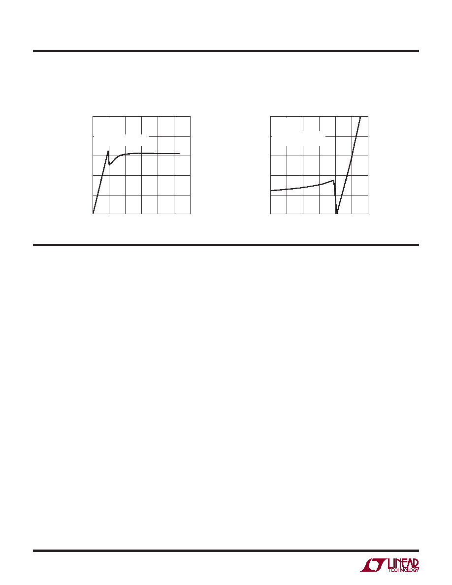
Short-Circuit Output Current vs
VOUT (Sinking)
Short-Circuit Output Current vs
VOUT (Sourcing)
1V/DIV
0
10mA/DIV
10
20
30
40
50
1
2
3
4
2607 G32
5
6
VCC = 5.5V
VREF = 5.6V
CODE = 0
VOUT SWEPT 0V TO VCC
1V/DIV
0
–50
10mA/DIV
–40
–30
–20
–10
0
1
2
3
4
2607 G33
5
6
VCC = 5.5V
VREF = 5.6V
CODE = FULL SCALE
VOUT SWEPT VCC TO 0V
LTC2607/LTC2617/LTC2627
typical perFormance characteristics
相关PDF资料 |
PDF描述 |
|---|---|
| VI-23B-IV-S | CONVERTER MOD DC/DC 95V 150W |
| VI-2NN-MW-F1 | CONVERTER MOD DC/DC 18.5V 100W |
| V150A36H400BF2 | CONVERTER MOD DC/DC 36V 400W |
| V150A36H400BL3 | CONVERTER MOD DC/DC 36V 400W |
| V150A36H400BL2 | CONVERTER MOD DC/DC 36V 400W |
相关代理商/技术参数 |
参数描述 |
|---|---|
| LTC2617IDE#PBF | 功能描述:IC DAC 14BIT R-R I2C 12-DFN RoHS:是 类别:集成电路 (IC) >> 数据采集 - 数模转换器 系列:- 标准包装:47 系列:- 设置时间:2µs 位数:14 数据接口:并联 转换器数目:1 电压电源:单电源 功率耗散(最大):55µW 工作温度:-40°C ~ 85°C 安装类型:表面贴装 封装/外壳:28-SSOP(0.209",5.30mm 宽) 供应商设备封装:28-SSOP 包装:管件 输出数目和类型:1 电流,单极;1 电流,双极 采样率(每秒):* |
| LTC2617IDE#TRPBF | 功能描述:IC DAC 14BIT R-R I2C 12-DFN RoHS:是 类别:集成电路 (IC) >> 数据采集 - 数模转换器 系列:- 标准包装:2,400 系列:- 设置时间:- 位数:18 数据接口:串行 转换器数目:3 电压电源:模拟和数字 功率耗散(最大):- 工作温度:-40°C ~ 85°C 安装类型:表面贴装 封装/外壳:36-TFBGA 供应商设备封装:36-TFBGA 包装:带卷 (TR) 输出数目和类型:* 采样率(每秒):* |
| LTC2617IDE-1#PBF | 功能描述:IC DAC 14BIT R-R I2C 12-DFN RoHS:是 类别:集成电路 (IC) >> 数据采集 - 数模转换器 系列:- 产品培训模块:LTC263x 12-, 10-, and 8-Bit VOUT DAC Family 特色产品:LTC2636 - Octal 12-/10-/8-Bit SPI VOUT DACs with 10ppm/°C Reference 标准包装:91 系列:- 设置时间:4µs 位数:10 数据接口:MICROWIRE?,串行,SPI? 转换器数目:8 电压电源:单电源 功率耗散(最大):2.7mW 工作温度:-40°C ~ 85°C 安装类型:表面贴装 封装/外壳:14-WFDFN 裸露焊盘 供应商设备封装:14-DFN-EP(4x3) 包装:管件 输出数目和类型:8 电压,单极 采样率(每秒):* |
| LTC2617IDE-1#TRPBF | 功能描述:IC DAC 14BIT R-R I2C 12-DFN RoHS:是 类别:集成电路 (IC) >> 数据采集 - 数模转换器 系列:- 标准包装:2,400 系列:- 设置时间:- 位数:18 数据接口:串行 转换器数目:3 电压电源:模拟和数字 功率耗散(最大):- 工作温度:-40°C ~ 85°C 安装类型:表面贴装 封装/外壳:36-TFBGA 供应商设备封装:36-TFBGA 包装:带卷 (TR) 输出数目和类型:* 采样率(每秒):* |
| LTC2619CGN#PBF | 功能描述:IC DAC 14BIT R-R QUAD 16SSOP RoHS:是 类别:集成电路 (IC) >> 数据采集 - 数模转换器 系列:- 标准包装:47 系列:- 设置时间:2µs 位数:14 数据接口:并联 转换器数目:1 电压电源:单电源 功率耗散(最大):55µW 工作温度:-40°C ~ 85°C 安装类型:表面贴装 封装/外壳:28-SSOP(0.209",5.30mm 宽) 供应商设备封装:28-SSOP 包装:管件 输出数目和类型:1 电流,单极;1 电流,双极 采样率(每秒):* |
发布紧急采购,3分钟左右您将得到回复。