参数资料
| 型号: | LTC2619IGN#PBF |
| 厂商: | Linear Technology |
| 文件页数: | 6/22页 |
| 文件大小: | 0K |
| 描述: | IC DAC 14BIT R-R QUAD 16SSOP |
| 标准包装: | 100 |
| 设置时间: | 9µs |
| 位数: | 14 |
| 数据接口: | 串行 |
| 转换器数目: | 4 |
| 电压电源: | 单电源 |
| 功率耗散(最大): | 750µW |
| 工作温度: | -40°C ~ 85°C |
| 安装类型: | 表面贴装 |
| 封装/外壳: | 16-SSOP(0.154",3.90mm 宽) |
| 供应商设备封装: | 16-SSOP |
| 包装: | 管件 |
| 输出数目和类型: | 4 电压,单极 |
| 采样率(每秒): | * |
LTC2609/LTC2619/LTC2629
26091929fb
operation
Power-On Reset
The LTC2609/LTC2619/LTC2629 clear the outputs to
zero-scale when power is first applied, making system
initialization consistent and repeatable. The LTC2609-1/
LTC2619-1/LTC2629-1setthevoltageoutputstomid-scale
when power is first applied.
Forsomeapplications,downstreamcircuitsareactivedur-
ingDACpower-upandmaybesensitivetononzerooutputs
from the DAC during this time. The LTC2609/LTC2619/
LTC2629 contain circuitry to reduce the power-on glitch;
furthermore, the glitch amplitude can be made arbitrarily
small by reducing the ramp rate of the power supply. For
example, if the power supply is ramped to 5V in 1ms, the
analog outputs rise less than 10mV above ground (typ)
during power-on. See Power-On Reset Glitch in the Typical
Performance Characteristics section.
Power Supply Sequencing
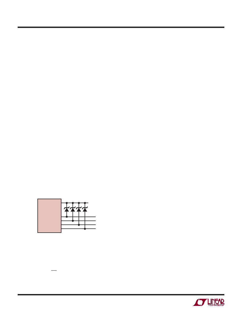
The voltage at REFx (Pins 3, 6, 12 and 15) should be kept
within the range –0.3V ≤ REFx ≤ VCC + 0.3V (see Absolute
Maximum Ratings). Particular care should be taken to
observe these limits during power supply turn-on and
turn-off sequences, when the voltage at VCC (Pin 16) is
in transition. The REFx pins can be clamped to stay below
the maximum voltage by using Schottky diodes as shown
in Figure 2, thereby easing sequencing constraints.
LTC2609/
LTC2619/
LTC2629
VCC
16
3
6
12
15
2609 F02
VCC
REFA
REFB
REFC
REFD
REFA
REFB
REFC
REFD
Figure 2. Use of Schottky Diodes for Power Supply Sequencing
Transfer Function
The digital-to-analog transfer function is:
V
k
REFx REFLO REFLO
OUT IDEAL
N
(
)
[
–
]
=
+
2
where k is the decimal equivalent of the binary DAC input
code, N is the resolution and REFx is the voltage at REFA,
REFB, REFC and REFD (Pins 3, 6, 12 and 15).
Serial Digital Interface
The LTC2609/LTC2619/LTC2629 communicate with a host
usingthestandard2-wireI2Cinterface.TheTimingDiagram
(Figure 1) shows the timing relationship of the signals on
the bus. The two bus lines, SDA and SCL, must be high
when the bus is not in use. External pull-up resistors or
current sources are required on these lines. The value of
thesepull-upresistorsisdependentonthepowersupplyand
can be obtained from the I2C specifications. For an I2C bus
operatinginthefastmode,anactivepull-upwillbenecessary
if the bus capacitance is greater than 200pF. The VCC power
shouldnotberemovedfromtheLTC2609/LTC2619/LTC2629
when the I2C bus is active to avoid loading the I2C bus lines
through the internal ESD protection diodes.
The LTC2609/LTC2619/LTC2629 are receive-only (slave)
devices. The master can write to the LTC2609/LTC2619/
LTC2629.TheLTC2609/LTC2619/LTC2629donotrespond
to a read from the master.
The START (S) and STOP (P) Conditions
Whenthebusisnotinuse,bothSCLandSDAmustbehigh.
A bus master signals the beginning of a communication
to a slave device by transmitting a START condition. A
START condition is generated by transitioning SDA from
high to low while SCL is high.
When the master has finished communicating with the
slave, it issues a STOP condition. A STOP condition is
generated by transitioning SDA from low to high while
SCL is high. The bus is then free for communication with
another I2C device.
Acknowledge
The Acknowledge signal is used for handshaking between
the master and the slave. An Acknowledge (active LOW)
generated by the slave lets the master know that the
latest byte of information was received. The Acknowledge
related clock pulse is generated by the master. The master
releasestheSDAline(HIGH)duringtheAcknowledgeclock
pulse. The slave-receiver must pull down the SDA bus line
相关PDF资料 |
PDF描述 |
|---|---|
| AD8307AR-REEL7 | IC LOGARITHMIC AMP 8-SOIC |
| VI-242-IV-F4 | CONVERTER MOD DC/DC 15V 150W |
| VI-242-IV-F3 | CONVERTER MOD DC/DC 15V 150W |
| 74LVC1G06FW4-7 | IC SGL INV GATE W/OD DFN1010-6 |
| VI-241-IV-F4 | CONVERTER MOD DC/DC 12V 150W |
相关代理商/技术参数 |
参数描述 |
|---|---|
| LTC2620CGN | 功能描述:IC DAC OCTAL R-R 12BIT 16SSOP RoHS:否 类别:集成电路 (IC) >> 数据采集 - 数模转换器 系列:- 标准包装:47 系列:- 设置时间:2µs 位数:14 数据接口:并联 转换器数目:1 电压电源:单电源 功率耗散(最大):55µW 工作温度:-40°C ~ 85°C 安装类型:表面贴装 封装/外壳:28-SSOP(0.209",5.30mm 宽) 供应商设备封装:28-SSOP 包装:管件 输出数目和类型:1 电流,单极;1 电流,双极 采样率(每秒):* |
| LTC2620CGN#PBF | 功能描述:IC DAC OCTAL R-R 12BIT 16SSOP RoHS:是 类别:集成电路 (IC) >> 数据采集 - 数模转换器 系列:- 产品培训模块:Lead (SnPb) Finish for COTS Obsolescence Mitigation Program 标准包装:50 系列:- 设置时间:4µs 位数:12 数据接口:串行 转换器数目:2 电压电源:单电源 功率耗散(最大):- 工作温度:-40°C ~ 85°C 安装类型:表面贴装 封装/外壳:8-TSSOP,8-MSOP(0.118",3.00mm 宽) 供应商设备封装:8-uMAX 包装:管件 输出数目和类型:2 电压,单极 采样率(每秒):* 产品目录页面:1398 (CN2011-ZH PDF) |
| LTC2620CGN#PBF | 制造商:Linear Technology 功能描述:D/A Converter (D-A) IC |
| LTC2620CGN#TR | 功能描述:IC DAC R-R 12-BIT OCTAL 16-SSOP RoHS:否 类别:集成电路 (IC) >> 数据采集 - 数模转换器 系列:- 标准包装:47 系列:- 设置时间:2µs 位数:14 数据接口:并联 转换器数目:1 电压电源:单电源 功率耗散(最大):55µW 工作温度:-40°C ~ 85°C 安装类型:表面贴装 封装/外壳:28-SSOP(0.209",5.30mm 宽) 供应商设备封装:28-SSOP 包装:管件 输出数目和类型:1 电流,单极;1 电流,双极 采样率(每秒):* |
| LTC2620CGN#TRPBF | 功能描述:IC DAC OCTAL R-R 12BIT 16SSOP RoHS:是 类别:集成电路 (IC) >> 数据采集 - 数模转换器 系列:- 标准包装:47 系列:- 设置时间:2µs 位数:14 数据接口:并联 转换器数目:1 电压电源:单电源 功率耗散(最大):55µW 工作温度:-40°C ~ 85°C 安装类型:表面贴装 封装/外壳:28-SSOP(0.209",5.30mm 宽) 供应商设备封装:28-SSOP 包装:管件 输出数目和类型:1 电流,单极;1 电流,双极 采样率(每秒):* |
发布紧急采购,3分钟左右您将得到回复。