- 您现在的位置:买卖IC网 > PDF目录8737 > LTC2621IDD#PBF (Linear Technology)IC DAC 12BIT SGL R-R VOUT 10DFN PDF资料下载
参数资料
| 型号: | LTC2621IDD#PBF |
| 厂商: | Linear Technology |
| 文件页数: | 16/16页 |
| 文件大小: | 0K |
| 描述: | IC DAC 12BIT SGL R-R VOUT 10DFN |
| 标准包装: | 121 |
| 设置时间: | 7µs |
| 位数: | 12 |
| 数据接口: | 串行 |
| 转换器数目: | 1 |
| 电压电源: | 单电源 |
| 功率耗散(最大): | 1.88mW |
| 工作温度: | -40°C ~ 85°C |
| 安装类型: | 表面贴装 |
| 封装/外壳: | 10-WFDFN 裸露焊盘 |
| 供应商设备封装: | 10-DFN(3x3) |
| 包装: | 管件 |
| 输出数目和类型: | 1 电压,单极 |
| 采样率(每秒): | * |
LTC2601/LTC2611/LTC2621
9
2601fb
PIN FUNCTIONS
SDO (Pin 1): Serial Interface Data Output. This pin is used
for daisy-chain operation. The serial output of the shift
register appears at the SDO pin. The data transferred to
the device via the SDI pin is delayed 32 SCK rising edges
before being output at the next falling edge. SDO is an
active output and does not go high impedance even when
CS/LD is taken to a logic high level.
SDI (Pin 2): Serial Interface Data Input. Data is applied
to SDI for transfer to the device at the rising edge of SCK
(Pin 3). The LTC2601 accepts input word lengths of either
24 or 32 bits.
SCK (Pin 3): Serial Interface Clock Input. CMOS and TTL
compatible.
CLR (Pin 4): Asynchronous Clear Input. A logic low at this
level-triggered input clears all registers and causes the
DAC voltage outputs to drop to 0V for LTC2601/LTC2611/
LTC2621. A logic low at this input sets all registers to
midscale code and causes the DAC voltage outputs to go
to midscale for LTC2601-1/LTC2611-1/LTC2621-1. CMOS
and TTL compatible.
CS/LD (Pin 5): Serial Interface Chip Select/Load Input.
When CS/LD is low, SCK is enabled for shifting data on
SDI into the register. When CS/LD is taken high, SCK
is disabled and the specied command (see Table 1) is
executed.
REF (Pin 6): Reference Voltage Input. 0V ≤ VREF ≤ VCC.
VOUT (Pin 7): DAC Analog Voltage Output. The output
range is 0V to VREF.
GND (Pin 8): Analog Ground.
VCC (Pin 9): Supply Voltage Input. 2.5V ≤ VCC ≤ 5.5V.
LDAC (Pin 10): Asynchronous DAC Update Pin. If CS/LD
is high, a falling edge on LDAC immediately updates the
DAC register with the contents of the input register (similar
to a software update). If CS/LD is low when LDAC goes
low, the DAC register is updated after CS/LD returns high.
A low on the LDAC pin powers up the DAC. A software
power down command is ignored if LDAC is low.
Exposed Pad (Pin 11): Ground. Must be soldered to PCB
ground.
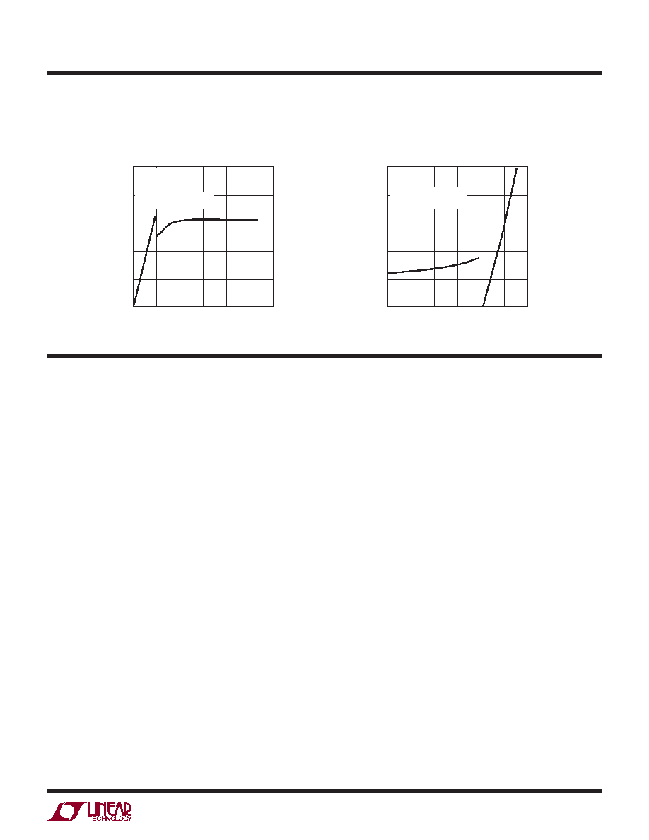
TYPICAL PERFORMANCE CHARACTERISTICS
Short-Circuit Output Current vs
VOUT (Sinking)
Short-Circuit Output Current vs
VOUT (Sourcing)
LTC2601/LTC2611/LTC2621
1V/DIV
0
10mA/DIV
10
20
30
40
50
1
23
4
2601 G15
56
VCC = 5.5V
VREF = 5.6V
CODE = 0
VOUT SWEPT 0V TO VCC
1V/DIV
0
–50
10mA/DIV
–40
–30
–20
–10
0
1
23
4
2601 G16
56
VCC = 5.5V
VREF = 5.6V
CODE = FULL SCALE
VOUT SWEPT VCC TO 0V
相关PDF资料 |
PDF描述 |
|---|---|
| AD5331BRUZ-REEL | IC DAC 10BIT SNGL VOUT 20-TSSOP |
| IDT2309NZ-1HDCG8 | IC CLOCK BUFFER 1:9 16-SOIC |
| VE-J64-MZ-F2 | CONVERTER MOD DC/DC 48V 25W |
| VI-21Z-MU-F1 | CONVERTER MOD DC/DC 2V 80W |
| VE-J63-MZ-F4 | CONVERTER MOD DC/DC 24V 25W |
相关代理商/技术参数 |
参数描述 |
|---|---|
| LTC-2621JD | 功能描述:LED 显示器和配件 3 Digit, Red Low Current RoHS:否 制造商:Avago Technologies 显示器类型:7 Segment 数位数量:2 字符大小:7.8 mm x 14.22 mm 照明颜色:Red 波长:628 nm 共用管脚:Common Anode 工作电压:2.05 V 工作电流:20 mA 最大工作温度:+ 85 C 最小工作温度:- 35 C 封装:Tube |
| LTC-2621JD-01 | 制造商:Lite-On Semiconductor Corporation 功能描述:DISPLAY,CLOCK,3-DIG,ALINGAP RED,LOW-CUR,0.28",CAMPX - Rail/Tube |
| LTC-2621P | 功能描述:LED 显示器和配件 3 Digit, Red RoHS:否 制造商:Avago Technologies 显示器类型:7 Segment 数位数量:2 字符大小:7.8 mm x 14.22 mm 照明颜色:Red 波长:628 nm 共用管脚:Common Anode 工作电压:2.05 V 工作电流:20 mA 最大工作温度:+ 85 C 最小工作温度:- 35 C 封装:Tube |
| LTC-2621WC | 功能描述:LED 显示器和配件 3 Digit, Red Low Current RoHS:否 制造商:Avago Technologies 显示器类型:7 Segment 数位数量:2 字符大小:7.8 mm x 14.22 mm 照明颜色:Red 波长:628 nm 共用管脚:Common Anode 工作电压:2.05 V 工作电流:20 mA 最大工作温度:+ 85 C 最小工作温度:- 35 C 封装:Tube |
| LTC-2621Y | 功能描述:LED 显示器和配件 3 Digit, Yellow RoHS:否 制造商:Avago Technologies 显示器类型:7 Segment 数位数量:2 字符大小:7.8 mm x 14.22 mm 照明颜色:Red 波长:628 nm 共用管脚:Common Anode 工作电压:2.05 V 工作电流:20 mA 最大工作温度:+ 85 C 最小工作温度:- 35 C 封装:Tube |
发布紧急采购,3分钟左右您将得到回复。