- 您现在的位置:买卖IC网 > PDF目录10783 > LTC2629IGN-1#TRPBF (Linear Technology)IC DAC 12BIT R-R QUAD 16SSOP PDF资料下载
参数资料
| 型号: | LTC2629IGN-1#TRPBF |
| 厂商: | Linear Technology |
| 文件页数: | 8/22页 |
| 文件大小: | 0K |
| 描述: | IC DAC 12BIT R-R QUAD 16SSOP |
| 标准包装: | 2,500 |
| 设置时间: | 7µs |
| 位数: | 12 |
| 数据接口: | 串行 |
| 转换器数目: | 4 |
| 电压电源: | 单电源 |
| 功率耗散(最大): | 750µW |
| 工作温度: | -40°C ~ 85°C |
| 安装类型: | 表面贴装 |
| 封装/外壳: | 16-SSOP(0.154",3.90mm 宽) |
| 供应商设备封装: | 16-SSOP |
| 包装: | 带卷 (TR) |
| 输出数目和类型: | 4 电压,单极 |
| 采样率(每秒): | * |
LTC2609/LTC2619/LTC2629
26091929fb
operation
loads a 16-bit data word from the 32-bit shift register
into the input register of the selected DAC, n. An update
operation copies the data word from the input register to
the DAC register. Once copied into the DAC register, the
data word becomes the active 16-, 14- or 12-bit input
code, and is converted to an analog voltage at the DAC
output. The update operation also powers up the selected
DAC if it had been in power-down mode. The data path
and registers are shown in the Block Diagram.
Power-Down Mode
Forpower-constrainedapplications,power-downmodecan
be used to reduce the supply current whenever less than
four outputs are needed. When in power-down, the buffer
amplifiers, bias circuits and reference inputs are disabled,
and draw essentially zero current. The DAC outputs are
put into a high impedance state, and the output pins are
passively pulled to REFLO through individual 90k resis-
tors. Input- and DAC-register contents are not disturbed
during power down.
Any channel or combination of channels can be put into
power-down mode by using command 0100b in combi-
nation with the appropriate DAC address, (n). The 16-bit
data word is ignored. The supply current is reduced by
approximately 1/4 for each DAC powered down. The effec-
tive resistance at REFx (Pins 3, 6, 12 and 15) are at high
impedance(typically>1GΩ)whenthecorrespondingDACs
are powered down. Normal operation can be resumed by
executing any command which includes a DAC update,
as shown in Table 2.
The selected DAC is powered up as its voltage output is
updated. When a DAC which is in a powered-down state
is powered up and updated, normal settling is delayed. If
less than four DACs are in a powered-down state prior to
the update command, the power-up delay time is 5s. If on
the other hand, all four DACs are powered down, then the
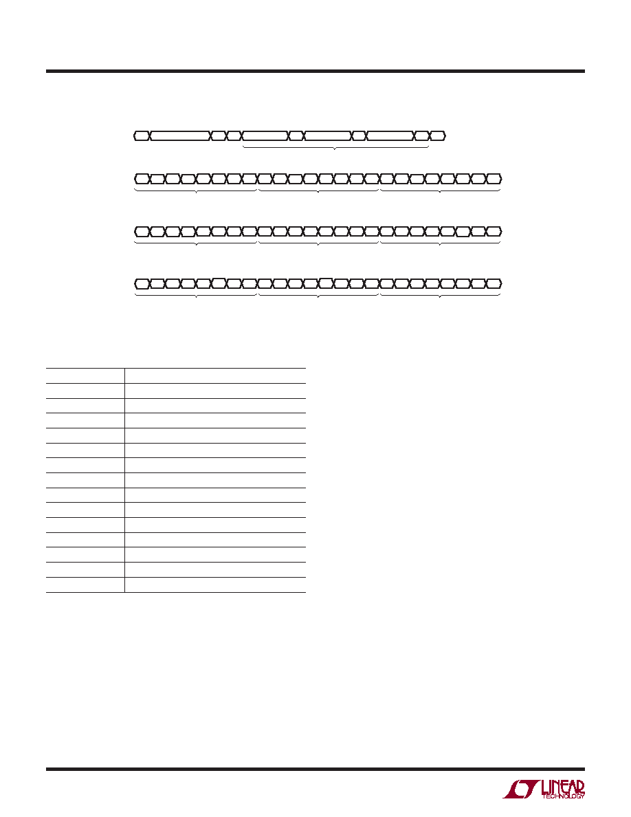
C3
1ST DATA BYTE
Input Word (LTC2609)
Write Word Protocol for LTC2609/LTC2619/LTC1629
C2 C1 C0 A3
D13
D14
D15
S
W
A
SLAVE ADDRESS
1ST DATA BYTE
D12 D11 D10 D9 D8 D7 D6 D5 D4 D3 D2 D1 D0
A
2ND DATA BYTE
A 3RD DATA BYTE
A
P
2609 F03
2ND DATA BYTE
INPUT WORD
3RD DATA BYTE
C3
1ST DATA BYTE
Input Word (LTC2619)
C2 C1 C0 A3
D11
D12
D13
D10 D9 D8 D7 D6 D5 D4 D3 D2 D1 D0
X
2ND DATA BYTE
3RD DATA BYTE
C3
1ST DATA BYTE
Input Word (LTC2629)
C2 C1 C0 A3
A2
A1
A0
D9
D10
D11
D8 D7 D6 D5 D4 D3 D2 D1 D0
X
2ND DATA BYTE
3RD DATA BYTE
Figure 3
Table 2
COMMAND*
C3 C2 C1 C0
0
0 Write to Input Register n
0
1 Update (Power Up) DAC Register n
0
1
0 Write to Input Register n, Update (Power Up) All n
0
1
1 Write to and Update (Power Up) n
0
1
0
0 Power Down n
1
1 No Operation
ADDRESS (n)*
A3 A2 A1 A0
0
0 DAC A
0
1 DAC B
0
1
0 DAC C
0
1
1 DAC D
1
1 All DACs
*Command and address codes not shown are reserved and should not be used.
相关PDF资料 |
PDF描述 |
|---|---|
| VI-JNN-MW-F2 | CONVERTER MOD DC/DC 18.5V 100W |
| LTC2629IGN#TRPBF | IC DAC 12BIT R-R QUAD 16SSOP |
| LTC2629CGN#TRPBF | IC DAC 12BIT R-R QUAD 16SSOP |
| LTC2617CDE-1#TRPBF | IC DAC 14BIT R-R I2C 12-DFN |
| VI-JNP-MW-F1 | CONVERTER MOD DC/DC 13.8V 100W |
相关代理商/技术参数 |
参数描述 |
|---|---|
| LTC2630ACSC6-HM12#PBF | 制造商:Linear Technology 功能描述:DAC 1-CH 12-bit 6-Pin SC-70 制造商:Linear Technology 功能描述:IC 12BIT DAC R/R INT REF SC70-6 制造商:Linear Technology 功能描述:IC, 12BIT DAC, R/R, INT REF, SC70-6 |
| LTC2630ACSC6-HM12#TRMPBF | 功能描述:IC DAC 12BIT R-R SC70-6 RoHS:是 类别:集成电路 (IC) >> 数据采集 - 数模转换器 系列:- 产品培训模块:Lead (SnPb) Finish for COTS Obsolescence Mitigation Program 标准包装:58 系列:- 设置时间:6µs 位数:8 数据接口:并联 转换器数目:4 电压电源:双 ± 功率耗散(最大):640mW 工作温度:-40°C ~ 85°C 安装类型:表面贴装 封装/外壳:24-SSOP(0.209",5.30mm 宽) 供应商设备封装:24-SSOP 包装:管件 输出数目和类型:4 电压,单极;4 电压,双极 采样率(每秒):* |
| LTC2630ACSC6-HM12#TRPBF | 功能描述:IC DAC 12BIT R-R SC70-6 RoHS:是 类别:集成电路 (IC) >> 数据采集 - 数模转换器 系列:- 产品培训模块:Lead (SnPb) Finish for COTS Obsolescence Mitigation Program 标准包装:58 系列:- 设置时间:6µs 位数:8 数据接口:并联 转换器数目:4 电压电源:双 ± 功率耗散(最大):640mW 工作温度:-40°C ~ 85°C 安装类型:表面贴装 封装/外壳:24-SSOP(0.209",5.30mm 宽) 供应商设备封装:24-SSOP 包装:管件 输出数目和类型:4 电压,单极;4 电压,双极 采样率(每秒):* |
| LTC2630ACSC6-HZ12#PBF | 制造商:Linear Technology 功能描述:IC 12BIT DAC R/R INT REF SC70-6 |
| LTC2630ACSC6-HZ12#TRMPBF | 功能描述:IC DAC 12BIT R-R SC70-6 RoHS:是 类别:集成电路 (IC) >> 数据采集 - 数模转换器 系列:- 产品培训模块:Lead (SnPb) Finish for COTS Obsolescence Mitigation Program 标准包装:58 系列:- 设置时间:6µs 位数:8 数据接口:并联 转换器数目:4 电压电源:双 ± 功率耗散(最大):640mW 工作温度:-40°C ~ 85°C 安装类型:表面贴装 封装/外壳:24-SSOP(0.209",5.30mm 宽) 供应商设备封装:24-SSOP 包装:管件 输出数目和类型:4 电压,单极;4 电压,双极 采样率(每秒):* |
发布紧急采购,3分钟左右您将得到回复。