- 您现在的位置:买卖IC网 > PDF目录21063 > LTC2630HSC6-HZ8#TRMPBF (Linear Technology)IC DAC 8BIT R-R SC70-6 PDF资料下载
参数资料
| 型号: | LTC2630HSC6-HZ8#TRMPBF |
| 厂商: | Linear Technology |
| 文件页数: | 6/22页 |
| 文件大小: | 0K |
| 描述: | IC DAC 8BIT R-R SC70-6 |
| 产品培训模块: | LTC263x 12-, 10-, and 8-Bit VOUT DAC Family |
| 标准包装: | 1 |
| 设置时间: | 3.2µs |
| 位数: | 8 |
| 数据接口: | 串行 |
| 转换器数目: | 1 |
| 电压电源: | 单电源 |
| 功率耗散(最大): | 480µW |
| 工作温度: | -40°C ~ 125°C |
| 安装类型: | 表面贴装 |
| 封装/外壳: | 6-TSSOP,SC-88,SOT-363 |
| 供应商设备封装: | SC-70-6 |
| 包装: | 标准包装 |
| 输出数目和类型: | 1 电压,单极 |
| 采样率(每秒): | * |
| 产品目录页面: | 1351 (CN2011-ZH PDF) |
| 其它名称: | LTC2630HSC6-HZ8#TRMPBFDKR |
LTC2630
14
2630ff
Serial Interface
The CS/LD input is level triggered. When this input is taken
low, it acts as a chip-select signal, enabling the SDI and
SCK buffers and the input shift register. Data (SDI input)
is transferred at the next 24 rising SCK edges. The 4-bit
command, C3-C0, is loaded first; then 4 don’t-care bits;
and finally the 16-bit data word. The data word comprises
the 12-, 10- or 8-bit input code, ordered MSB-to-LSB, fol-
lowed by 4, 6 or 8 don’t-care bits (LTC2630-12, -10 and
-8 respectively; see Figure 2). Data can only be transferred
to the device when the CS/LD signal is low, beginning on
the first rising edge of SCK. SCK may be high or low at
the falling edge of CS/LD. The rising edge of CS/LD ends
the data transfer and causes the device to execute the
command specified in the 24-bit input sequence. The
complete sequence is shown in Figure 3a.
operation
The command (C3-C0) assignments are shown in Table 1.
The first three commands in the table consist of write and
update operations. A Write operation loads a 16-bit data
word from the 24-bit shift register into the input register.
In an Update operation, the input register is copied to the
DAC register and converted to an analog voltage at the
DAC output. Write to and Update combines the first two
commands. The Update operation also powers up the
DAC if it had been in power-down mode. The data path
and registers are shown in the Block Diagram.
While the minimum input sequence is 24-bits, it may
optionally be extended to 32-bits to accommodate micro-
processors that have a minimum word width of 16-bits
(2 bytes). To use the 32-bit width, 8 don’t-care bits are
transferred to the device first, followed by the 24-bit se-
quence described. Figure 3b shows the 32-bit sequence.
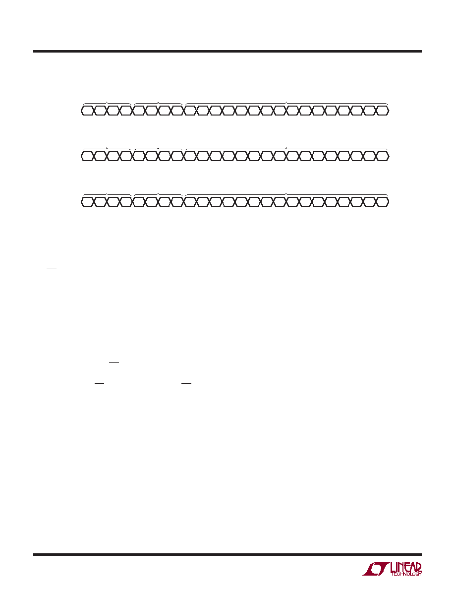
2630 F02
C3
COMMAND
4 DON'T-CARE BITS
MSB
LSB
DATA (12 BITS + 4 DON'T-CARE BITS)
C2
C1
C0
X
D11 D10 D9
D8
D7
D6
D5
D4
D3
D2
D1
D0
X
C3
COMMAND
4 DON'T-CARE BITS
DATA (10 BITS + 6 DON'T-CARE BITS)
C2
C1
C0
X
D9
D8
D7
D6
D5
D4
D3
D2
D1
D0
X
C3
COMMAND
INPUT WORD (LTC2630-12)
INPUT WORD (LTC2630-10)
INPUT WORD (LTC2630-8)
4 DON'T-CARE BITS
DATA (8 BITS + 8 DON'T-CARE BITS)
C2
C1
C0
X
D7
D6
D5
D4
D3
D2
D1
D0
X
Figure 2. Command and Data Input Format
相关PDF资料 |
PDF描述 |
|---|---|
| P51-3000-A-M-P-5V-000-000 | SENSOR 3000PSI M10-1.0 6G 1-5V |
| P51-2000-A-R-MD-5V-000-000 | SENSOR 2000PSI M12-1.0 6G 1-5V |
| P51-1000-S-Y-MD-4.5OVP-000-000 | SENSOR 1000PSI 7/16-20-2B 4.5V |
| REC5-4812DRWZ/H2/A/M/SMD-R | CONV DC/DC 5W 18-72VIN +/-12VOUT |
| P51-50-G-G-I36-4.5V-000-000 | SENSOR 50PSI 1/8-27NPT .5-4.5V |
相关代理商/技术参数 |
参数描述 |
|---|---|
| LTC2630HSC6-LM10#TRMPBF | 功能描述:IC DAC 10BIT R-R SC70-6 RoHS:是 类别:集成电路 (IC) >> 数据采集 - 数模转换器 系列:- 产品培训模块:Lead (SnPb) Finish for COTS Obsolescence Mitigation Program 标准包装:58 系列:- 设置时间:6µs 位数:8 数据接口:并联 转换器数目:4 电压电源:双 ± 功率耗散(最大):640mW 工作温度:-40°C ~ 85°C 安装类型:表面贴装 封装/外壳:24-SSOP(0.209",5.30mm 宽) 供应商设备封装:24-SSOP 包装:管件 输出数目和类型:4 电压,单极;4 电压,双极 采样率(每秒):* |
| LTC2630HSC6-LM10#TRPBF | 功能描述:IC DAC 10BIT R-R SC70-6 RoHS:是 类别:集成电路 (IC) >> 数据采集 - 数模转换器 系列:- 产品培训模块:Data Converter Fundamentals DAC Architectures 设计资源:Unipolar, Precision DC Digital-to-Analog Conversion using AD5450/1/2/3 8-14-Bit DACs (CN0052) Precision, Bipolar, Configuration for AD5450/1/2/3 8-14bit Multiplying DACs (CN0053) AC Signal Processing Using AD5450/1/2/3 Current Output DACs (CN0054) Programmable Gain Element Using AD5450/1/2/3 Current Output DAC Family (CN0055) Single Supply Low Noise LED Current Source Driver Using a Current Output DAC in the Reverse Mode (CN0139) 标准包装:10,000 系列:- 设置时间:- 位数:12 数据接口:DSP,MICROWIRE?,QSPI?,串行,SPI? 转换器数目:1 电压电源:单电源 功率耗散(最大):- 工作温度:-40°C ~ 125°C 安装类型:表面贴装 封装/外壳:SOT-23-8 薄型,TSOT-23-8 供应商设备封装:TSOT-23-8 包装:带卷 (TR) 输出数目和类型:1 电流,单极;1 电流,双极 采样率(每秒):2.7M |
| LTC2630HSC6-LM12#PBF | 制造商:Linear Technology 功能描述:DAC 1-CH 12-bit 6-Pin SC-70 制造商:Linear Technology 功能描述:IC 12BIT DAC R/R INT REF SC70-6 |
| LTC2630HSC6-LM12#TRMPBF | 功能描述:IC DAC 12BIT R-R SC70-6 RoHS:是 类别:集成电路 (IC) >> 数据采集 - 数模转换器 系列:- 产品培训模块:Lead (SnPb) Finish for COTS Obsolescence Mitigation Program 标准包装:58 系列:- 设置时间:6µs 位数:8 数据接口:并联 转换器数目:4 电压电源:双 ± 功率耗散(最大):640mW 工作温度:-40°C ~ 85°C 安装类型:表面贴装 封装/外壳:24-SSOP(0.209",5.30mm 宽) 供应商设备封装:24-SSOP 包装:管件 输出数目和类型:4 电压,单极;4 电压,双极 采样率(每秒):* |
| LTC2630HSC6-LM12#TRPBF | 功能描述:IC DAC 12BIT R-R SC70-6 RoHS:是 类别:集成电路 (IC) >> 数据采集 - 数模转换器 系列:- 产品培训模块:Data Converter Fundamentals DAC Architectures 设计资源:Unipolar, Precision DC Digital-to-Analog Conversion using AD5450/1/2/3 8-14-Bit DACs (CN0052) Precision, Bipolar, Configuration for AD5450/1/2/3 8-14bit Multiplying DACs (CN0053) AC Signal Processing Using AD5450/1/2/3 Current Output DACs (CN0054) Programmable Gain Element Using AD5450/1/2/3 Current Output DAC Family (CN0055) Single Supply Low Noise LED Current Source Driver Using a Current Output DAC in the Reverse Mode (CN0139) 标准包装:10,000 系列:- 设置时间:- 位数:12 数据接口:DSP,MICROWIRE?,QSPI?,串行,SPI? 转换器数目:1 电压电源:单电源 功率耗散(最大):- 工作温度:-40°C ~ 125°C 安装类型:表面贴装 封装/外壳:SOT-23-8 薄型,TSOT-23-8 供应商设备封装:TSOT-23-8 包装:带卷 (TR) 输出数目和类型:1 电流,单极;1 电流,双极 采样率(每秒):2.7M |
发布紧急采购,3分钟左右您将得到回复。