参数资料
| 型号: | LTC2642IMS-16#TRPBF |
| 厂商: | Linear Technology |
| 文件页数: | 4/24页 |
| 文件大小: | 0K |
| 描述: | IC DAC 16BIT VOUT 10-MSOP |
| 标准包装: | 2,500 |
| 设置时间: | 1µs |
| 位数: | 16 |
| 数据接口: | 串行 |
| 转换器数目: | 1 |
| 电压电源: | 单电源 |
| 功率耗散(最大): | 600µW |
| 工作温度: | -40°C ~ 85°C |
| 安装类型: | 表面贴装 |
| 封装/外壳: | 10-TFSOP,10-MSOP(0.118",3.00mm 宽) |
| 供应商设备封装: | 10-MSOP |
| 包装: | 带卷 (TR) |
| 输出数目和类型: | 1 电压,单极;1 电压,双极 |
| 采样率(每秒): | * |
LTC2641/LTC2642
12
26412fc
For more information www.linear.com/LTC2641
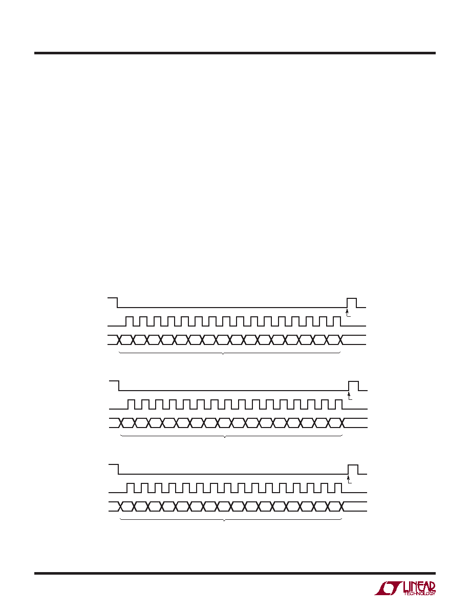
operaTion
high-to-low transition, the data on DIN is loaded, MSB
first, into the shift register on each rising edge of the serial
clock input (SCLK). After 16 data bits have been loaded
into the serial input register, a low-to-high transition on
CS transfers the data to the 16-bit DAC latch, updating
the DAC output (see Figures 1a, 1b, 1c). While CS remains
high, the serial input shift register is disabled. If there
are less than 16 low-to-high transitions on SCLK while
CS remains low, the data will be corrupted, and must be
reloaded.Also,iftherearemorethan16low-to-hightransi-
tions on SCLK while CS remains low, only the last 16 data
bits loaded from DIN will be transferred to the DAC latch.
For the 14-bit DACs, (LTC2641-14/LTC2642-14), the MSB
remains in the same (left-justified) position in the input
16-bit data word. Therefore, two “don’t-care” bits must
be loaded after the LSB, to make up the required 16 data
bits (Figure 1b). Similarly, for the 12-bit family members
(LTC2641-12/LTC2642-12) four “don’t-care” bits must
follow the LSB (Figure 1c).
Power-On Reset
The LTC2641/LTC2642 include a power-on reset circuit
to ensure that the DAC ouput comes up in a known state.
When VDD is first applied, the power-on reset circuit
sets the output of the LTC2641 to zero-scale (code 0).
The LTC2642 powers up to midscale (bipolar zero). De-
pending on the DAC number of bits, the midscale code
is: 32,768 (LTC2642-16); 8,192 (LTC2642-14); or 2,048
(LTC2642-12).
Clearing the DAC
A 10ns (minimum) low pulse on the CLR pin asynchro-
nously clears the DAC latch to code zero (LTC2641) or to
midscale (LTC2642).
Figure 1c. 12-Bit Timing Diagram (LTC2641-12/LTC2642-12)
Figure 1b. 14-Bit Timing Diagram (LTC2641-14/LTC2642-14)
Figure 1a. 16-Bit Timing Diagram (LTC2641-16/LTC2642-16)
D15
MSB
1
CS
SCLK
DIN
2
3
4
5
6
7
8
9
10
11
12
13
14
15
16
D14 D13 D12 D11 D10 D9
D8
DATA (16 BITS)
D7
D6
D5
D4
D3
D2
D1
D0
DAC
UPDATED
LSB
26412 F01a
D13
MSB
1
CS
SCLK
DIN
2
3
4
5
6
7
8
9
10
11
12
13
14
15
16
D12 D11 D10 D9
D8
D7
D6
DATA (14 BITS + 2 DON’T-CARE BITS)
D5
D4
D3
D2
D1
D0
X
DAC
UPDATED
LSB
26412 F01b
MSB
1
CS
SCLK
DIN
2
3
4
5
6
7
8
9
10
11
12
13
14
15
16
D11 D10 D9
D8
D7
D6
DATA (12 BITS + 4 DON’T-CARE BITS)
D5
D4
D3
D2
D1
D0
X
DAC
UPDATED
LSB
26412 F01c
相关PDF资料 |
PDF描述 |
|---|---|
| LTC1446LIN8 | IC D/A CONV 12BIT R-R DUAL 8-DIP |
| VI-210-IV-F2 | CONVERTER MOD DC/DC 5V 150W |
| MC10E111FNR2 | IC CLK BUFFER 1:9 800MHZ 28-PLCC |
| LTC2642IDD-16#TRPBF | IC DAC 16BIT VOUT 10-DFN |
| LTC2641IMS8-16#TRPBF | IC DAC 16BIT VOUT 8-MSOP |
相关代理商/技术参数 |
参数描述 |
|---|---|
| LTC-2651TBE-01 | 制造商:LITEON 功能描述:8*4 ND, 0.28 inch, common anode, color-blue |
| LTC2654BCGN-H16#PBF | 功能描述:IC DAC 16BITS SER 16SSOP RoHS:是 类别:集成电路 (IC) >> 数据采集 - 数模转换器 系列:- 标准包装:1 系列:- 设置时间:4.5µs 位数:12 数据接口:串行,SPI? 转换器数目:1 电压电源:单电源 功率耗散(最大):- 工作温度:-40°C ~ 125°C 安装类型:表面贴装 封装/外壳:8-SOIC(0.154",3.90mm 宽) 供应商设备封装:8-SOICN 包装:剪切带 (CT) 输出数目和类型:1 电压,单极;1 电压,双极 采样率(每秒):* 其它名称:MCP4921T-E/SNCTMCP4921T-E/SNRCTMCP4921T-E/SNRCT-ND |
| LTC2654BCGN-H16#TRPBF | 功能描述:IC DAC 16BIT SRL 16SSOP RoHS:是 类别:集成电路 (IC) >> 数据采集 - 数模转换器 系列:- 产品培训模块:Data Converter Fundamentals DAC Architectures 标准包装:750 系列:- 设置时间:7µs 位数:16 数据接口:并联 转换器数目:1 电压电源:双 ± 功率耗散(最大):100mW 工作温度:0°C ~ 70°C 安装类型:表面贴装 封装/外壳:28-LCC(J 形引线) 供应商设备封装:28-PLCC(11.51x11.51) 包装:带卷 (TR) 输出数目和类型:1 电压,单极;1 电压,双极 采样率(每秒):143k |
| LTC2654BCGN-L16#PBF | 功能描述:IC DAC 16BITS SER 16SSOP RoHS:是 类别:集成电路 (IC) >> 数据采集 - 数模转换器 系列:- 标准包装:1 系列:- 设置时间:4.5µs 位数:12 数据接口:串行,SPI? 转换器数目:1 电压电源:单电源 功率耗散(最大):- 工作温度:-40°C ~ 125°C 安装类型:表面贴装 封装/外壳:8-SOIC(0.154",3.90mm 宽) 供应商设备封装:8-SOICN 包装:剪切带 (CT) 输出数目和类型:1 电压,单极;1 电压,双极 采样率(每秒):* 其它名称:MCP4921T-E/SNCTMCP4921T-E/SNRCTMCP4921T-E/SNRCT-ND |
| LTC2654BCGN-L16#TRPBF | 功能描述:IC DAC 16BIT SRL 16SSOP RoHS:是 类别:集成电路 (IC) >> 数据采集 - 数模转换器 系列:- 产品培训模块:Data Converter Fundamentals DAC Architectures 标准包装:750 系列:- 设置时间:7µs 位数:16 数据接口:并联 转换器数目:1 电压电源:双 ± 功率耗散(最大):100mW 工作温度:0°C ~ 70°C 安装类型:表面贴装 封装/外壳:28-LCC(J 形引线) 供应商设备封装:28-PLCC(11.51x11.51) 包装:带卷 (TR) 输出数目和类型:1 电压,单极;1 电压,双极 采样率(每秒):143k |
发布紧急采购,3分钟左右您将得到回复。