- 您现在的位置:买卖IC网 > PDF目录179918 > LTC2846CG#TR (LINEAR TECHNOLOGY CORP) 3.3V Software-Selectable Multiprotocol Transceiver with Termination; Package: SSOP; No of Pins: 36; Temperature Range: 0°C to +70°C PDF资料下载
参数资料
| 型号: | LTC2846CG#TR |
| 厂商: | LINEAR TECHNOLOGY CORP |
| 元件分类: | Buffer和线驱动 |
| 英文描述: | 3.3V Software-Selectable Multiprotocol Transceiver with Termination; Package: SSOP; No of Pins: 36; Temperature Range: 0°C to +70°C |
| 中文描述: | TRIPLE LINE TRANSCEIVER, PDSO36 |
| 封装: | 0.209 INCH, PLASTIC, SSOP-36 |
| 文件页数: | 8/24页 |
| 文件大小: | 278K |
| 代理商: | LTC2846CG#TR |
16
LTC2846
sn2846 2846fs
APPLICATIO S I FOR ATIO
WU
UU
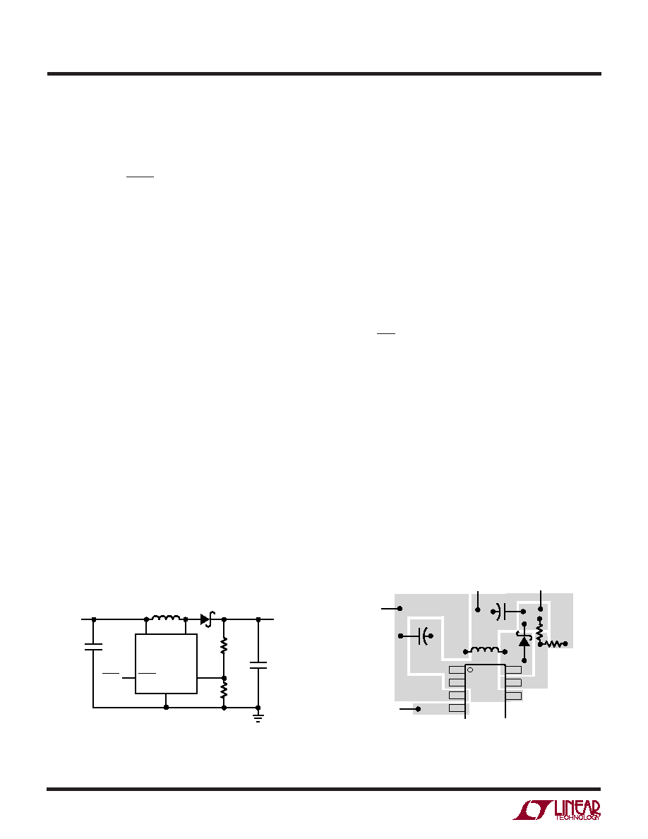
Switching Regulator
The circuit as shown in Figure 29 can provide up to 480mA
at 5V to drive the LTC2846’s transceiver as well as its
companion chip in the DTE-DCE interface. In its shut down
mode with the SHDN pin at 0V, the boost switching
regulator draws less than 10
A.
Ferrite core inductors should be used to obtain the best
efficiency, as core losses at 1.2MHz are much lower for
ferrite cores than for cheaper powdered-iron types. Choose
an inductor that can handle at least 1A without saturating,
and ensure that the inductor has a low DCR (copper wire
resistance) to minimize I2R power losses.
Use low ESR capacitors for the output to minimize output
ripple voltage. Multilayer ceramic capacitors are an excel-
lent choice, as they have extremely low ESR and are
available in very small packages. Ceramic capacitors also
make a good choice for the input decoupling capacitor,
and should be placed as close as possible to the switching
regulator. Solid tantalum or OS-CON capacitors can be
used but they will occupy more board area than a ceramic
and will have a higher ESR.
A Schottky diode is recommended for use with the switch-
ing regulator. The ON Semiconductor MBR0520 is a very
good choice.
To set the output voltage, select the values of R1 and R2
according to the following equation.
R1 = R2[(5V/1.255V) – 1]
A good value for R2 is 4.3k which sets the current in the
resistor divider chain to 1.255V/4.3k = 292
A.
The switching regulator has a switch current limit of 1A.
This current limit protects the switch as well as the exter-
nal components connected to the switching regulator.
The high speed operation of the boost switching regulator
demands careful attention to board layout. Figure 30
shows the recommended component placement.
Receiver Fail-Safe
All LTC2846/LTC2844 receivers feature fail-safe opera-
tion in all modes. If the receiver inputs are left floating or
are shorted together by a termination resistor, the receiver
output will always be forced to a logic high.
DTE vs DCE Operation
The DCE/DTE pin acts as an enable for Driver 3/Receiver 1
in the LTC2846, and Driver 3/Receiver 1 and Receiver 4/
Driver 4 in the LTC2844.
The LTC2846/LTC2844 can be configured for either DTE
or DCE operation in one of two ways: a dedicated DTE or
DCE port with a connector of appropriate gender or a port
with one connector that can be configured for DTE or DCE
operation by rerouting the signals to the LTC2846/LTC2844
using a dedicated DTE cable or dedicated DCE cable.
A dedicated DTE port using a DB-25 male connector is
shown in Figure 31. The interface mode is selected by logic
outputs from the controller or from jumpers to either VIN
or GND on the mode select pins. A dedicated DCE port
using a DB-25 female connector is shown in Figure 32.
GND
VIN
SW
SHDN
FB
VIN
3.3V
4
35
2846 F29
D1
L1
5.6
H
2, 34
R1
13k
BOOST
SWITCHING
REGULATOR
C5
10
F
C6
10
F
R2
4.3k
VCC
5V
480mA
C5,C6: TAIYO YUDEN X5R JMK316BJ106ML
D1: ON SEMICONDUCTOR MBR0520
L1: SUMIDA CR43-5R6
SHDN
336
R1
R2
2846 F30
GND
L1
VCC
VIN
SHUTDOWN
+
C6
D1
+
C5
Figure 29. Boost Switching Regulator
Figure 30. Suggested Layout
相关PDF资料 |
PDF描述 |
|---|---|
| LTC2847CUHF#TR | Software-Selectable Multiprotocol Transceiver with Termination and 3.3V Digital Interface; Package: QFN; No of Pins: 38; Temperature Range: 0°C to +70°C |
| LTC4252-2CMS#TRPBF | Negative Voltage Hot Swap Controllers; Package: MSOP; No of Pins: 10; Temperature Range: 0°C to +70°C |
| LTC4252-2IMS#PBF | Negative Voltage Hot Swap Controllers; Package: MSOP; No of Pins: 10; Temperature Range: -40°C to +85°C |
| LTC4252-2IMS#TRPBF | Negative Voltage Hot Swap Controllers; Package: MSOP; No of Pins: 10; Temperature Range: -40°C to +85°C |
| LTC4252A-1CMS#PBF | Negative Voltage Hot Swap Controllers; Package: MSOP; No of Pins: 10; Temperature Range: 0°C to +70°C |
相关代理商/技术参数 |
参数描述 |
|---|---|
| LTC2846IG | 功能描述:IC TXRX 3.3V MULTIPROTCOL 36SSOP RoHS:否 类别:集成电路 (IC) >> 接口 - 驱动器,接收器,收发器 系列:- 标准包装:250 系列:- 类型:收发器 驱动器/接收器数:2/2 规程:RS232 电源电压:3 V ~ 5.5 V 安装类型:表面贴装 封装/外壳:16-TSSOP(0.173",4.40mm 宽) 供应商设备封装:16-TSSOP 包装:带卷 (TR) |
| LTC2846IG#PBF | 功能描述:IC TXRX 3.3V MULTIPROTCOL 36SSOP RoHS:是 类别:集成电路 (IC) >> 接口 - 驱动器,接收器,收发器 系列:- 产品培训模块:RS-232 & USB Transceiver 标准包装:2,000 系列:- 类型:收发器 驱动器/接收器数:1/1 规程:RS232 电源电压:3 V ~ 5.5 V 安装类型:表面贴装 封装/外壳:16-SSOP(0.209",5.30mm 宽) 供应商设备封装:16-SSOP 包装:带卷 (TR) 其它名称:296-19849-2 |
| LTC2846IG#TR | 功能描述:IC TXRX 3.3V MULTIPROTCOL 36SSOP RoHS:否 类别:集成电路 (IC) >> 接口 - 驱动器,接收器,收发器 系列:- 标准包装:250 系列:- 类型:收发器 驱动器/接收器数:2/2 规程:RS232 电源电压:3 V ~ 5.5 V 安装类型:表面贴装 封装/外壳:16-TSSOP(0.173",4.40mm 宽) 供应商设备封装:16-TSSOP 包装:带卷 (TR) |
| LTC2846IG#TRPBF | 功能描述:IC TXRX 3.3V MULTIPROTCOL 36SSOP RoHS:是 类别:集成电路 (IC) >> 接口 - 驱动器,接收器,收发器 系列:- 标准包装:250 系列:- 类型:收发器 驱动器/接收器数:2/2 规程:RS232 电源电压:3 V ~ 5.5 V 安装类型:表面贴装 封装/外壳:16-TSSOP(0.173",4.40mm 宽) 供应商设备封装:16-TSSOP 包装:带卷 (TR) |
| LTC2847CUHF | 功能描述:IC TXRX MULTIPROTOCOL 38-QFN RoHS:否 类别:集成电路 (IC) >> 接口 - 驱动器,接收器,收发器 系列:- 标准包装:250 系列:- 类型:收发器 驱动器/接收器数:2/2 规程:RS232 电源电压:3 V ~ 5.5 V 安装类型:表面贴装 封装/外壳:16-TSSOP(0.173",4.40mm 宽) 供应商设备封装:16-TSSOP 包装:带卷 (TR) |
发布紧急采购,3分钟左右您将得到回复。