参数资料
| 型号: | LTC3025EDC#TR |
| 厂商: | Linear Technology |
| 文件页数: | 5/12页 |
| 文件大小: | 0K |
| 描述: | IC REG LDO ADJ .3A 6DFN |
| 标准包装: | 2,500 |
| 稳压器拓扑结构: | 正,可调式 |
| 输出电压: | 0.4 V ~ 3.6 V |
| 输入电压: | 0.9 V ~ 5.5 V |
| 电压 - 压降(标准): | 0.045V @ 300mA |
| 稳压器数量: | 1 |
| 电流 - 输出: | 300mA(最小) |
| 工作温度: | -40°C ~ 125°C |
| 安装类型: | 表面贴装 |
| 封装/外壳: | 6-WFDFN 裸露焊盘 |
| 供应商设备封装: | 6-DFN-EP(2x2) |
| 包装: | 带卷 (TR) |
�� �
�
�LTC3025�
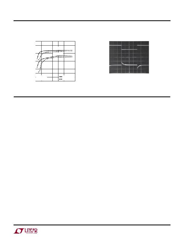
�TYPICAL� PERFORMANCE� CHARACTERISTICS�
�50�
�3MHz� V� IN� Supply� Rejection�
�Transient� Response�
�45�
�40�
�35�
�C� OUT� = 10μF�
�C� OUT� = 1μF�
�I� OUT�
�250mA�
�10mA�
�30�
�25�
�20�
�15�
�V� OUT�
�AC�
�10mV/DIV�
�10�
�5� V� BIAS� =� 3.6V�
�V� OUT� =� 1.2V�
�0�
�1.2� 1.4� 1.6�
�1.8�
�2.0�
�I� OUT� =� 100mA�
�I� OUT� =� 300mA�
�2.2� 2.4� 2.6�
�V� IN� =� 1.5V�
�V� OUT� =� 1.2V�
�V� BIAS� =� 3.6V�
�C� OUT� =� 1μF�
�100μs/DIV�
�3025� G13�
�V� IN� (V)�
�3025� G12�
�PIN� FUNCTIONS�
�BIAS� (Pin� 1):� BIAS� Input� Voltage.� BIAS� provides� internal�
�power� for� LTC3025� circuitry.� The� BIAS� pin� should� be� lo-�
�cally� bypassed� to� ground� if� the� LTC3025� is� more� than� a�
�few� inches� away� from� another� source� of� bulk� capacitance.�
�In� general,� the� output� impedance� of� a� battery� rises� with�
�frequency,� so� it� is� usually� advisable� to� include� an� input�
�bypass� capacitor� in� battery-powered� circuits.� A� capacitor�
�in� the� range� of� 0.01μF� to� 0.1μF� is� usually� suf?cient.�
�GND� (Pin� 2):� Ground.� Connect� to� a� ground� plane.�
�IN� (Pin� 3):� Input� Supply� Voltage.� The� output� load� current�
�is� supplied� directly� from� IN.� The� IN� pin� should� be� locally�
�bypassed� to� ground� if� the� LTC3025� is� more� than� a� few� inches�
�away� from� another� source� of� bulk� capacitance.� In� general,�
�the� output� impedance� of� a� battery� rises� with� frequency,� so�
�it� is� usually� advisable� to� include� an� input� bypass� capacitor�
�when� supplying� IN� from� a� battery.� A� capacitor� in� the� range�
�of� 0.1μF� to� 1μF� is� usually� suf?cient.�
�OUT� (Pin� 4):� Regulated� Output� Voltage.� The� OUT� pin�
�capacitor� of� at� least� 1μF� is� required� to� ensure� stability.�
�Larger� output� capacitors� may� be� required� for� applications�
�with� large� transient� loads� to� limit� peak� voltage� transients.�
�See� the� Applications� Information� section� for� more� informa-�
�tion� on� output� capacitance.�
�ADJ� (Pin� 5):� Adjust� Input.� This� is� the� input� to� the� error�
�ampli?er.� The� ADJ� pin� reference� voltage� is� 0.4V� referenced�
�to� ground.� The� output� voltage� range� is� 0.4V� to� 3.6V� and� is�
�typically� set� by� connecting� ADJ� to� a� resistor� divider� from�
�OUT� to� GND.� See� Figure� 2.�
�SHDN� (Pin� 6):� Shutdown� Input,� Active� Low.� This� pin� is�
�used� to� put� the� LTC3025� into� shutdown.� The� SHDN� pin�
�current� is� typically� less� than� 10nA.� The� SHDN� pin� cannot�
�be� left� ?oating� and� must� be� tied� to� a� valid� logic� level� (such�
�as� BIAS)� if� not� used.�
�GND� (Exposed� Pad� Pin� 7):� Ground� and� Heat� Sink.� Must�
�be� soldered� to� PCB� ground� plane� or� large� pad� for� optimal�
�thermal� performance.�
�supplies� power� to� the� load.� A� minimum� ceramic� output�
�3025fd�
�5�
�相关PDF资料 |
PDF描述 |
|---|---|
| MIC39150-2.5WU TR | IC REG LDO 2.5V 1.5A TO-263 |
| RSM22DTMN-S189 | CONN EDGECARD 44POS R/A .156 SLD |
| LT3060EDC-5#TRPBF | IC REG LDO 5V .1A 8DFN |
| LT3060EDC-3.3#TRPBF | IC REG LDO 3.3V .1A 8DFN |
| LT3060EDC-2.5#TRPBF | IC REG LDO 2.5V .1A 8DFN |
相关代理商/技术参数 |
参数描述 |
|---|---|
| LTC3025EDC-TRPBF | 制造商:LINER 制造商全称:Linear Technology 功能描述:300mA Micropower VLDO Linear Regulator |
| LTC3025IDC | 制造商:LINER 制造商全称:Linear Technology 功能描述:300mA Micropower VLDO Linear Regulator |
| LTC3025IDC#PBF | 制造商:Linear Technology 功能描述:LDO 5.5V 0.045VDO 0.3A 6DFN 制造商:Linear Technology 功能描述:LDO, 5.5V, 0.045VDO, 0.3A, 6DFN 制造商:Linear Technology 功能描述:DP-LINREG, Cut Tape 200mA Micropower VLDO Linear Regulator |
| LTC3025IDC#TRMPBF | 功能描述:IC REG LDO ADJ .3A 6-DFN RoHS:是 类别:集成电路 (IC) >> PMIC - 稳压器 - 线性 系列:- 产品培训模块:More Information on LDOs 标准包装:50 系列:- 稳压器拓扑结构:正,固定式 输出电压:3.3V 输入电压:最高 15V 电压 - 压降(标准):1.1V @ 800mA 稳压器数量:1 电流 - 输出:800mA 电流 - 限制(最小):800mA 工作温度:0°C ~ 125°C 安装类型:表面贴装 封装/外壳:TO-263-4,D²Pak(3 引线+接片),TO-263AA 供应商设备封装:D2PAK-3 包装:管件 |
| LTC3025IDC#TRPBF | 功能描述:IC REG LDO ADJ .3A 6-DFN RoHS:是 类别:集成电路 (IC) >> PMIC - 稳压器 - 线性 系列:- 产品培训模块:More Information on LDOs 标准包装:50 系列:- 稳压器拓扑结构:正,固定式 输出电压:3.3V 输入电压:最高 15V 电压 - 压降(标准):1.1V @ 800mA 稳压器数量:1 电流 - 输出:800mA 电流 - 限制(最小):800mA 工作温度:0°C ~ 125°C 安装类型:表面贴装 封装/外壳:TO-263-4,D²Pak(3 引线+接片),TO-263AA 供应商设备封装:D2PAK-3 包装:管件 |
发布紧急采购,3分钟左右您将得到回复。