- 您现在的位置:买卖IC网 > PDF目录20628 > LTC3104IDE#TRPBF (Linear Technology)IC REG DL BUCK/LINEAR SYNC 14DFN PDF资料下载
参数资料
| 型号: | LTC3104IDE#TRPBF |
| 厂商: | Linear Technology |
| 文件页数: | 14/20页 |
| 文件大小: | 339K |
| 描述: | IC REG DL BUCK/LINEAR SYNC 14DFN |
| 标准包装: | 2,500 |
| 拓扑: | 降压(降压)同步(1),线性(LDO)(1) |
| 功能: | 任何功能 |
| 输出数: | 2 |
| 频率 - 开关: | 1.2MHz |
| 电压/电流 - 输出 1: | 0.6 V ~ 13.8 V,300mA |
| 电压/电流 - 输出 2: | 0.6 V ~ 14.5 V,10mA |
| 带 LED 驱动器: | 无 |
| 带监控器: | 无 |
| 带序列发生器: | 无 |
| 电源电压: | 2.5 V ~ 15 V |
| 工作温度: | -40°C ~ 125°C |
| 安装类型: | 表面贴装 |
| 封装/外壳: | 14-WFDFN 裸露焊盘 |
| 供应商设备封装: | 14-DFN(4x3) |
| 包装: | 带卷 (TR) |
LTC3104
14
3104f
Input Capacitor Selection
The V
IN
and V
INLDO
pins provide current to the power
stages of the buck converter and the LDO, respectively.
It is recommended that a low ESR ceramic capacitor with
a value of at least 10礔 be used to bypass each of these
pins. These capacitors should be placed as close to the
respective pin as possible and should have a short return
path to the GND pin.
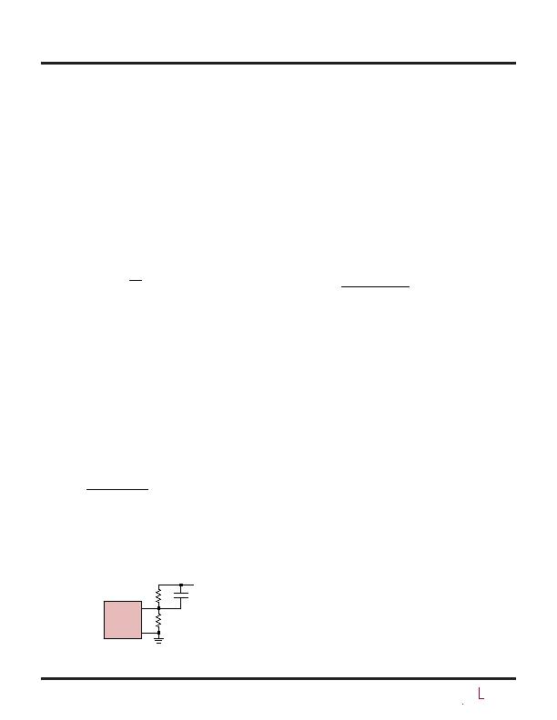
Output Voltage Programming
The output voltage is set by a resistive divider according
to the following formula:
V
OUT
=0.6V 1+
R2
R1
?/DIV>
?/DIV>
?/DIV>
?/DIV>
?/DIV>
?/DIV>
The external divider is connected to the output as shown
in Figure 1. Note that FB divider current is not included in
the LTC3104 quiescent current specification. For improved
transient response, a feedforward capacitor, C
FF
, may be
placed in parallel with resistor R2. The capacitor modifies
the loop dynamics by adding a pole-zero pair to the loop
dynamics which generates a phase boost that can improve
the phase margin and increase the speed of the transient
response, resulting in smaller voltage deviation on load
transients. The zero frequency depends not only on the
value of the feed forward capacitor, but also on the upper
resistor divider resistor. Specifically, the zero frequency,
f
ZERO
, is given by the following equation:
f
ZERO
=
1
2 ?R2 C
FF1
For R2 resistor values of ~1M a 12pF ceramic capacitor
will suffice, however that value may be increased or de-
creased to optimize the converters response for a given
set of application parameters.
APPLICATIONS INFORMATION
Figure 1. Setting the Output Voltage
FB
R2
R1
C
FF1
3104 F01
V
OUT
GND
LTC3104
Minimum Off-Time/On-Time Considerations
The maximum duty cycle is limited in the LTC3104 by the
boost capacitor refresh time, the rise/fall times of the switch
as well as propagation delays in the PWM comparator, the
level shifts and the gate drive. This minimum off-time is
typically 65ns which imposes a maximum duty cycle of:
DC
MAX
= 1 (f " t
OFF(MIN)
)
where f is the 1.2MHz switching frequency and t
OFF(MIN)
is the minimum off-time. If the maximum duty cycle is
surpassed, due to a dropping input voltage for example,
the output will drop out of regulation. The minimum input
voltage to avoid this dropout condition is:
V
IN(MIN)
=
V
OUT
1 f t
OFF(MIN)
(
)
Conversely, the minimum on-time is the smallest duration
of time in which the buck switch can be in its
on
state.
This time is limited by similar factors and is typically 70ns.
In forced continuous operation, the minimum on-time limit
imposes a minimum duty cycle of:
DC
MIN
= f " t
ON(MIN)
where t
ON(MIN)
is the minimum on-time. In extreme step-
down ratios where the minimum duty cycle is surpassed,
the output voltage will still be in regulation but the rectifier
switch will remain on for more than one cycle and sub-
harmonic switching will occur to provide a higher effective
duty cycle. The result is higher output voltage ripple. This is
an acceptable result in many applications so this constraint
may not be of critical importance in some cases.
Precise Undervoltage Lockout
The LTC3104 is in shutdown when the RUN pin is low and
active when the pin is higher than the RUN pin threshold.
The rising threshold of the RUN pin comparator is an
accurate 0.8V, with 60mV of hysteresis. This threshold is
enabled when V
IN
is above the 2.5V minimum value. If V
IN
is lower than 2.5V, an internal undervoltage monitor puts
the part in shutdown independent of the RUN pin state.
The RUN pin can be configured as a precise undervoltage
lockout (UVLO) on the V
IN
supply with a resistive divider
tied to the RUN pin as shown in Figure 2 to meet specific
相关PDF资料 |
PDF描述 |
|---|---|
| GBM15DCCD | CONN EDGECARD 30POS R/A .156 SLD |
| LT3570EUF#PBF | IC REG TRPL BCK/BST/LINEAR 24QFN |
| TH3C476K010C0500 | CAP TANT 47UF 10V 10% 2312 |
| LTC3104IMSE#PBF | IC REG DL BCK/LINEAR SYNC 16MSOP |
| SS3P6-E3/85A | DIODE SCHOTTKY 3A 60V SMP |
相关代理商/技术参数 |
参数描述 |
|---|---|
| LTC3104IMSE#PBF | 功能描述:IC REG DL BCK/LINEAR SYNC 16MSOP RoHS:是 类别:集成电路 (IC) >> PMIC - 稳压器 - 线性 + 切换式 系列:- 标准包装:2,500 系列:- 拓扑:降压(降压)同步(3),线性(LDO)(2) 功能:任何功能 输出数:5 频率 - 开关:300kHz 电压/电流 - 输出 1:控制器 电压/电流 - 输出 2:控制器 电压/电流 - 输出 3:控制器 带 LED 驱动器:无 带监控器:无 带序列发生器:是 电源电压:5.6 V ~ 24 V 工作温度:-40°C ~ 85°C 安装类型:* 封装/外壳:* 供应商设备封装:* 包装:* |
| LTC3104IMSE#TRPBF | 功能描述:IC REG DL BCK/LINEAR SYNC 16MSOP RoHS:是 类别:集成电路 (IC) >> PMIC - 稳压器 - 线性 + 切换式 系列:- 标准包装:2,500 系列:- 拓扑:降压(降压)同步(3),线性(LDO)(2) 功能:任何功能 输出数:5 频率 - 开关:300kHz 电压/电流 - 输出 1:控制器 电压/电流 - 输出 2:控制器 电压/电流 - 输出 3:控制器 带 LED 驱动器:无 带监控器:无 带序列发生器:是 电源电压:5.6 V ~ 24 V 工作温度:-40°C ~ 85°C 安装类型:* 封装/外壳:* 供应商设备封装:* 包装:* |
| LTC3105 | 制造商:LINER 制造商全称:Linear Technology 功能描述:400mA Step-Up DC/DC Converter with Maximum Power Point Control and 250mV Start-Up |
| LTC3105EDD#PBF | 功能描述:IC CONV DC/DC 400MA HIEFF 10-DFN RoHS:是 类别:集成电路 (IC) >> PMIC - 稳压器 - 专用型 系列:- 标准包装:43 系列:- 应用:控制器,Intel VR11 输入电压:5 V ~ 12 V 输出数:1 输出电压:0.5 V ~ 1.6 V 工作温度:-40°C ~ 85°C 安装类型:表面贴装 封装/外壳:48-VFQFN 裸露焊盘 供应商设备封装:48-QFN(7x7) 包装:管件 |
| LTC3105EDD#TRPBF | 功能描述:IC CONV DC/DC 400MA HIEFF 10-DFN RoHS:是 类别:集成电路 (IC) >> PMIC - 稳压器 - 专用型 系列:- 标准包装:43 系列:- 应用:控制器,Intel VR11 输入电压:5 V ~ 12 V 输出数:1 输出电压:0.5 V ~ 1.6 V 工作温度:-40°C ~ 85°C 安装类型:表面贴装 封装/外壳:48-VFQFN 裸露焊盘 供应商设备封装:48-QFN(7x7) 包装:管件 |
发布紧急采购,3分钟左右您将得到回复。