- 您现在的位置:买卖IC网 > PDF目录20847 > LTC3202EMS#PBF (Linear Technology)IC LED DRVR WHITE BCKLGT 10-MSOP PDF资料下载
参数资料
| 型号: | LTC3202EMS#PBF |
| 厂商: | Linear Technology |
| 文件页数: | 7/12页 |
| 文件大小: | 0K |
| 描述: | IC LED DRVR WHITE BCKLGT 10-MSOP |
| 标准包装: | 50 |
| 拓扑: | PWM,切换式电容器(充电泵) |
| 输出数: | 1 |
| 内部驱动器: | 是 |
| 类型 - 主要: | 背光 |
| 类型 - 次要: | 白色 LED |
| 频率: | 1.5MHz |
| 电源电压: | 2.7 V ~ 4.5 V |
| 安装类型: | 表面贴装 |
| 封装/外壳: | 10-TFSOP,10-MSOP(0.118",3.00mm 宽) |
| 供应商设备封装: | 10-MSOP |
| 包装: | 管件 |
| 工作温度: | -40°C ~ 85°C |
�� �
�
�LTC3202�
�OPERATIO�
�(Refer� to� Simplified� Block� Diagram)�
�In� this� configuration� the� feedback� factor� (� ?� V� FB� /� ?� V� OUT� )� will�
�be� very� near� unity� since� the� small� signal� LED� impedance�
�will� be� considerably� less� than� the� current� setting� resistor�
�R� X� .� Thus,� this� configuration� will� have� the� highest� loop� gain�
�giving� it� the� lowest� closed-loop� output� resistance.� Like-�
�wise� it� will� also� require� the� largest� amount� of� output�
�capacitance� to� preserve� stability.�
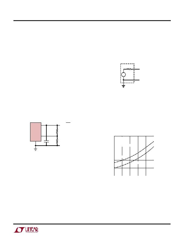
�Charge� Pump� Strength�
�Figure� 3� shows� how� the� LTC3202� can� be� modeled� as� a�
�Thevenin� equivalent� circuit� to� determine� the� amount� of�
�current� available� from� the� effective� input� voltage,� 1.5V� IN�
�and� the� effective� open-loop� output� resistance,� R� OL� .�
�For� fixed� voltage� applications,� the� output� voltage� can� be�
�set� by� the� ratio� of� two� resistors� and� the� feedback� control�
�R� OL�
�+�
�voltage� as� shown� in� Figure� 2.� The� output� voltage� is� given�
�+�
�–�
�1.5V� IN�
�V� OUT�
�by� the� set� point� voltage� times� the� gain� factor� 1� +� R� 1� /R� 2� .�
�Note� that� the� closed-loop� output� resistance� will� increase� in�
�proportion� to� the� loop� gain� consumed� by� the� resistive�
�divider� ratio.� For� example,� if� the� resistor� ratio� is� 2:1� giving�
�a� gain� of� 3,� the� closed-loop� output� resistance� will� be� about�
�3� times� higher� than� its� nominal� gain� of� 1� value.� Given� that�
�the� closed-loop� output� resistance� is� about� 0.35� ?� with� a�
�–�
�3202� F03�
�Figure� 3.� Equivalent� Open-Loop� Circuit�
�From� Figure� 3� the� available� current� is� given� by:�
�gain� of� 1,� the� closed-loop� output� resistance� will� be� about�
�1� ?� when� using� a� gain� of� 3.�
�I� OUT� =�
�1.5 V� IN� – V� OUT�
�R� OL�
�V� OUT�
�3�
�V� OUT� =� V� FB� (1� +�
�R1�
�R2�
�)�
�Typical� values� of� R� OL� as� a� function� of� temperature� are�
�shown� in� Figure� 4.�
�LTC3202�
�R1�
�FB�
�GND�
�5,� 11�
�2�
�1� μ� F�
�R2�
�4.8�
�4.6�
�V� FB� =� 0�
�I� L� =� 100mA�
�C1� =� C2� =� 1� μ� F�
�R� OL� =� (1.5V� IN� –� V� OUT� )/I� L�
�3202� F02�
�4.4�
�Figure� 2.� Voltage� Control� Mode�
�When� using� the� LTC3202� in� voltage� control� mode,� any� of�
�the� three� voltage� settings� (0.2V,� 0.4V� or� 0.6V)� can� be� used�
�4.2�
�4.0�
�V� IN� = 2.7V�
�V� IN� = 3.6V�
�as� the� set� point� voltage.� For� optimum� noise� performance�
�and� lowest� closed-loop� output� resistance� the� highest�
�voltage� setting� will� likely� be� the� most� desirable.�
�3.8�
�–40�
�–15�
�10� 35�
�TEMPERATURE� (� °� C)�
�60�
�85�
�3202� F04�
�Typical� values� for� total� voltage� divider� resistance� can�
�range� from� several� k� ?� s� up� to� 1M� ?� .�
�Figure� 4.� Typical� R� OL� vs� Temperature�
�3202fa�
�7�
�相关PDF资料 |
PDF描述 |
|---|---|
| LTC3202EMS | IC LED DRVR WHITE BCKLGT 10-MSOP |
| LTC3201EMS#PBF | IC LED DRVR WHITE BCKLGT 10-MSOP |
| VLCF4020T-6R8N1R0 | INDUCTOR POWER 6.8UH 1.0A SMD |
| P51-3000-S-M-I12-4.5V-000-000 | SENSOR 3000PSI M10-1.0 6G 4.5V |
| REC5-2409SRW/H2/C/M/SMD-R | CONV DC/DC 5W 18-36VIN 09VOUT |
相关代理商/技术参数 |
参数描述 |
|---|---|
| LTC3203 | 制造商:LINER 制造商全称:Linear Technology 功能描述:500mA Output Current Low Noise Dual Mode Step-Up Charge Pumps |
| LTC3203-1 | 制造商:LINER 制造商全称:Linear Technology 功能描述:500mA Output Current Low Noise Dual Mode Step-Up Charge Pumps |
| LTC3203B | 制造商:LINER 制造商全称:Linear Technology 功能描述:500mA Output Current Low Noise Dual Mode Step-Up Charge Pumps |
| LTC3203B-1 | 制造商:LINER 制造商全称:Linear Technology 功能描述:500mA Output Current Low Noise Dual Mode Step-Up Charge Pumps |
| LTC3203BEDD | 制造商:LINER 制造商全称:Linear Technology 功能描述:500mA Output Current Low Noise Dual Mode Step-Up Charge Pumps |
发布紧急采购,3分钟左右您将得到回复。