- 您现在的位置:买卖IC网 > PDF目录14832 > LTC3203EDD-1#PBF (Linear Technology)IC REG BOOST SWITCHED CAP 10DFN PDF资料下载
参数资料
| 型号: | LTC3203EDD-1#PBF |
| 厂商: | Linear Technology |
| 文件页数: | 11/16页 |
| 文件大小: | 0K |
| 描述: | IC REG BOOST SWITCHED CAP 10DFN |
| 标准包装: | 121 |
| 类型: | 升压(升压),切换电容(充电泵) |
| 输出类型: | 固定 |
| 输出数: | 1 |
| 输出电压: | 4.5V |
| 输入电压: | 2.7 V ~ 5.5 V |
| PWM 型: | Burst Mode? |
| 频率 - 开关: | 900kHz,1MHz |
| 电流 - 输出: | 500mA |
| 同步整流器: | 无 |
| 工作温度: | -40°C ~ 85°C |
| 安装类型: | 表面贴装 |
| 封装/外壳: | 10-WFDFN 裸露焊盘 |
| 包装: | 管件 |
| 供应商设备封装: | 10-DFN(3x3) |
�� �
�
�LTC3203/LTC3203-1�
�LTC3203B/LTC3203B-1�
�APPLICATIO� S� I� FOR� ATIO�
�V� IN� MODEL� ?� ?� MODE� 1� +� 1� ?�
�=� V�
�1� .� 5� ?� V� MODEL� ?� ?� MODE� 1� +� 1� ?�
�resistorR� X� .Thus,thisconfigurationwillhavethehighest�
�loop� gain� giving� it� the� lowest� closed-loop� output� resis-�
�tance.� Likewise� it� will� also� require� the� largest� amount� of�
�output� capacitance� to� preserve� stability.�
�Effective� Open� Loop� Output� Resistance� (R� OL� )�
�The� effective� open� loop� output� resistance� (R� OL� )� of� a�
�charge� pump� is� a� very� important� parameter,� which� deter-�
�mines� its� strength.� The� value� of� this� parameter� depends� on�
�many� factors� such� as� the� oscillator� frequency� (f� OSC� ),� the�
�value� of� the� flying� capacitor� (C� FLY� ),� the� non-overlap� time,�
�the� internal� switch� resistances� (R� S� ),� and� the� ESR� of� the�
�external� capacitors.�
�Maximum� Available� Output� Current�
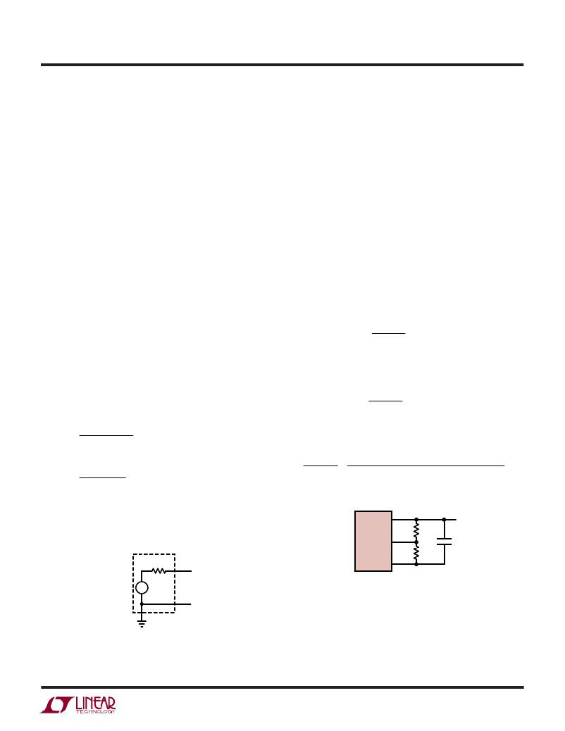
�Figure� 3� shows� how� the� LTC3203/LTC3203-1/LTC3203B/�
�LTC3203B-1� can� be� modeled� as� a� Thevenin-equivalent�
�circuit.�
�Thus� the� maximum� available� output� current� and� voltage�
�can� be� calculated� from� the� effective� open-loop� output�
�resistance,� R� OL� ,� and� the� effective� output� voltage,� 1.5V� IN�
�(in� 1.5x� mode)� or� 2V� IN� (in� 2x� mode).� From� Figure� 3,� the�
�available� current� is� given� by:�
�Programming� the� MODE� Pin�
�By� connecting� a� resistor� divider� to� the� MODE� pin,� the� V� IN�
�voltage� at� which� the� chip� switches� modes� can� be� accu-�
�rately� programmed.�
�When� V� IN� ramps� up,� the� voltage� at� the� MODE� pin� crosses�
�V� MODEH� and� the� chip� switches� from� 2x� mode� to� 1.5x� mode.�
�When� V� IN� starts� to� drop,� the� voltage� at� the� MODE� pin�
�crosses� V� MODEL� and� the� chip� switches� back� to� 2x� mode.�
�The� MODE� pin� resistor� ratio� must� be� selected� such� that� at�
�the� switch� point� the� output� is� still� able� to� maintain� regula-�
�tion� at� maximum� I� OUT� :�
�1.5� ?� V� IN(1.5x)� –� V� OUT� >� I� OUT� ?� R� OL(1.5X)�
�The� minimum� V� IN� operating� in� 1.5x� mode� occurs� at� the�
�switch� point� where:�
�?� R� ?�
�?� R� MODE� 2� ?�
�therefore:�
�?� R� ?�
�?� R� MODE� 2� ?�
�R� MODE� 1� V� OUT� (� M� I� N� )� +� R� OL� (� 1� .� 5� x� )(� MAX� )� ?� I� OUT� (� MAX� )�
�I� OUT� =�
�I� OUT� =�
�1.5 V� IN� ?� V� OUT�
�R� OL�
�2 V� IN� ?� V� OUT�
�R� OL�
�In� 1� .� 5� x� mod� e�
�In� 2� x� mod� e�
�>� R� OL� (� 1� .� 5� X� )(� M� A� X� )� ?� I� OUT� (� MAX� )� +� V� OUT� (� MIN� )�
�>�
�R� MODE� 2� 1� .� 5� ?� V� MODEL�
�–� 1�
�As� evident� from� the� above� two� equations,� with� the� same�
�V� IN� and� R� OL� ,� the� 2x� mode� will� give� more� output� current�
�than� the� 1.5x� mode.�
�V� IN�
�LTC3203/�
�LTC3203B�
�MODE�
�7�
�6�
�R� MODE1�
�C� IN�
�R� MODE2�
�1.5V� IN�
�OR�
�2V� IN�
�+�
�–�
�R� OL�
�+�
�V� OUT�
�GND�
�9,� 11�
�Figure� 4�
�3203� F04�
�–�
�3203� F03�
�Figure� 3.� Charge� Pump� Open-Loop� Thevenin-Equivalent� Circuit�
�32031fa�
�11�
�相关PDF资料 |
PDF描述 |
|---|---|
| ECM36DRKI-S13 | CONN EDGECARD 72POS .156 EXTEND |
| ABM15DRYN-S13 | CONN EDGECARD EXTEND 30POS .156 |
| GEM44DRKI | CONN EDGECARD 88POS DIP .156 SLD |
| ABM15DRYH-S13 | CONN EDGECARD EXTEND 30POS .156 |
| MAX6406BS33+T | IC DETECTOR VOLT 4-UCSP |
相关代理商/技术参数 |
参数描述 |
|---|---|
| LTC3204 | 制造商:LINER 制造商全称:Linear Technology 功能描述:Low Noise Regulated Charge Pump in 2 X 2 DFN |
| LTC3204-3.3 | 制造商:LINER 制造商全称:Linear Technology 功能描述:Low Noise Regulated Charge Pump in 2 X 2 DFN |
| LTC3204-5 | 制造商:LINER 制造商全称:Linear Technology 功能描述:Low Noise Regulated Charge Pump in 2 X 2 DFN |
| LTC3204B-3.3 | 制造商:LINER 制造商全称:Linear Technology 功能描述:Low Noise Regulated Charge Pump in 2 X 2 DFN |
| LTC3204B-5 | 制造商:LINER 制造商全称:Linear Technology 功能描述:Low Noise Regulated Charge Pump in 2 X 2 DFN |
发布紧急采购,3分钟左右您将得到回复。